Rising Demand for Advanced Chips
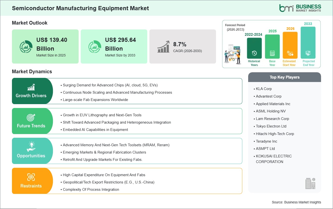
The rising demand for advanced chips is fundamentally reshaping the semiconductor manufacturing equipment market, as AI acceleration, high-performance computing (HPC), and next-generation edge devices push fabrication requirements beyond traditional limits. AI workloads—across data centers, foundation model training clusters, generative AI inference systems, and specialized accelerators—require chips with massive transistor counts, advanced interconnect architectures, and extremely high energy efficiency. To meet these demands, semiconductor manufacturers are aggressively pursuing smaller technology nodes, such as 5nm, 3nm, and 2nm, as well as novel transistor designs like GAAFETs and nanosheet architectures. This shift places intense pressure on equipment suppliers to deliver lithography, deposition, etching, and metrology systems capable of producing features at atomic-scale precision. Moreover, AI and HPC chips often employ complex 3D stacking, high-bandwidth memory interfaces, and advanced packaging technologies, all of which require sophisticated tools for wafer bonding, TSV formation, micro-bumping, and inspection. As AI training clusters continue to scale, the push for faster GPU, TPU, and custom AI accelerators drives unprecedented capital expenditure in advanced fabs—directly fueling strong growth in the semiconductor manufacturing equipment market.
Rapid Adoption of EUV and Next-Generation Lithography
The semiconductor industry’s drive toward smaller process nodes, particularly sub-3nm technology, is significantly accelerating the adoption of extreme ultraviolet (EUV) lithography and other next-generation lithography techniques. As chipmakers seek higher transistor density, improved performance, and lower power consumption, conventional lithography tools are becoming insufficient. This shift compels manufacturers to invest heavily in advanced lithography equipment, including EUV scanners, photomasks, optics, and supporting metrology and inspection systems. The complexity of these tools, combined with the precision required at sub-3nm nodes, creates strong, sustained demand for high-end semiconductor manufacturing equipment. Moreover, the adoption of EUV and advanced lithography not only drives volume demand for new machines but also creates a ripple effect across the semiconductor manufacturing equipment ecosystem. Equipment vendors supplying deposition, etching, chemical-mechanical planarization (CMP), and inspection tools must upgrade their technologies to maintain compatibility with EUV processes. This results in a multi-faceted growth opportunity, as fabs upgrading to next-generation nodes require complete production lines with fully integrated advanced tools.