
Wafer Vacuum Assembling Equipment Market Outlook: Size, Share, Trends, Growth Analysis, Competitive Landscape & Forecast, 2026–2033

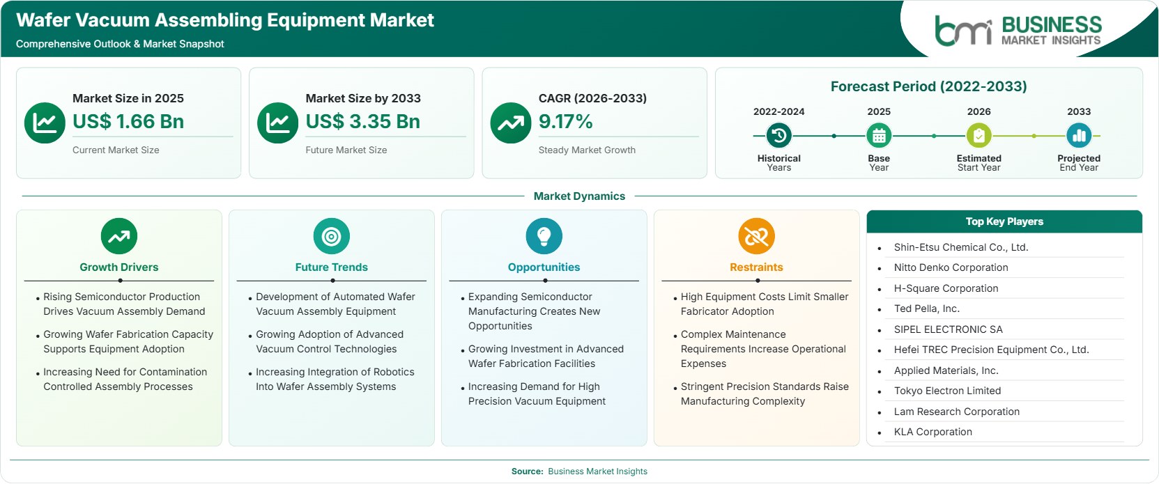
The Wafer Vacuum Assembling Equipment Market size was valued at US$ 1.66 Billion in 2025 and is projected to reach US$ 3.35 Billion by 2033, growing at a CAGR of 9.17% during 2026–2033, driven by semiconductor capacity expansion, advanced packaging, contamination control, precision bonding, and wafer-level manufacturing.

Report Coverage
  • Equipment Type: Wafer Bonding Equipment, Wafer Alignment Systems, Vacuum Handling & Transfer Systems, Wafer Packaging/Encapsulation Equipment, Others
  • End User: Semiconductor Foundries, Integrated Device Manufacturers , OSAT, MEMS & Sensors Manufacturers, Power Electronics
  • Wafer Size: Below 200mm, 200-300mm, Above 300mm
US$ 1.66 Bn Market size in 2025
US$ 3.35 Bn Market Size by 2033
9.17% CAGR, 2026 - 2033
2026-2033 Forecast Period

AI Overview

Wafer Vacuum Assembling Equipment Market Summary

  • North America: North America holds a 24%–27% share in 2025 and is growing at a 8.1%–9.0% CAGR through 2033, supported by semiconductor reshoring, advanced packaging investments, foundry expansion, and demand for contamination-controlled assembly. The US accounts for a 20%–23% of North American share and is advancing at a 8.3%–9.2% CAGR, supported by fab investments, advanced packaging, and domestic semiconductor manufacturing initiatives.
  • Fastest Growing Region: Asia Pacific holds a 47%–51% share in 2025 and is advancing at a 10.0%–11.0% CAGR, supported by expanding wafer fabrication capacity, advanced packaging investments, foundry development, semiconductor localization programs, and rising demand for high-precision vacuum assembly equipment.
  • Leading Segment: Wafer Bonding Equipment accounts for a 32%–36% share in 2025 and is advancing at a 9.5%–10.4% CAGR, supported by heterogeneous integration, MEMS manufacturing, advanced packaging, thin-wafer processing, and growing requirements for precise contamination-controlled bonding.
  • High Growth Segment: Above 300mm wafer applications represent a 12%–16% share in 2025 and are advancing at a 10.2%–11.2% CAGR, supported by high-volume semiconductor manufacturing, larger wafer economics, advanced process integration, and demand for automated precision handling.
  • Key Market Opportunity: Expansion of advanced semiconductor fabs creates opportunities for integrated vacuum assembly platforms combining bonding, alignment, handling, automation, inspection, process monitoring, and contamination control within connected production environments.
  • Major Market Players: Shin-Etsu Chemical Co., Ltd., Nitto Denko Corporation, H-Square Corporation, Ted Pella, Inc., SIPEL ELECTRONIC SA, Hefei TREC Precision Equipment Co., Ltd., Applied Materials, Inc., Tokyo Electron Limited, Lam Research Corporation, KLA Corporation
Strategic Insights

Wafer Vacuum Assembling Equipment Market: Strategic Insights

Wafer Vacuum Assembling Equipment Market Strategic Framework
FREE PDF
Request your free sample
Request free sample
Stakeholder View

Key Takeaways

  • Advanced wafer bonding and assembly processes are becoming increasingly important as semiconductor architectures incorporate thinner wafers, heterogeneous materials, and more complex packaging structures.
  • Equipment suppliers can capture higher-value opportunities by combining vacuum handling, wafer alignment, bonding, encapsulation, automation, and process monitoring within integrated manufacturing platforms.
  • Contamination control remains a fundamental purchasing consideration because microscopic particles, surface defects, and bonding inconsistencies can compromise downstream semiconductor and MEMS yields.
  • Asia Pacific provides the strongest expansion opportunity because established semiconductor manufacturing clusters are being complemented by new fabrication and packaging capacity.
  • Equipment purchasing decisions increasingly consider lifecycle economics, including uptime, maintenance requirements, automation capability, process repeatability, upgradeability, and technical service availability.
  • Long-term competitive positioning will depend on the ability to support advanced wafer sizes, heterogeneous integration, high-throughput production, precise alignment, and increasingly automated manufacturing environments.
Geographic Outlook

Wafer Vacuum Assembling Equipment Market Regional Highlights

North America Wafer Vacuum Assembling Equipment Market

North America holds a 24%–27% share in 2025 and is projected to grow at an 8.1%–9.0% CAGR through 2033. The need for local manufacturing chains, the reshoring of semiconductors, additional fabrication facilities, and advanced packaging initiatives is reinforcing equipment needs throughout the region.

  • Investments in semiconductor manufacturing are generating a rise in the demand for precise wafer handling, bonding, aligning, and vacuum-compatible assembling systems.
  • The development of advanced packaging is creating demands for sophisticated assembly methods that can accommodate thin wafers and complex devices.
  • Buyers of equipment are looking for automation, process control, contamination control, and service responsiveness in order to enhance reliability and utilization of equipment.
  • The United States continues to be the prime demand center, whereas Canada and Mexico offer supportive business prospects through electronics manufacturing and the semiconductor supply chain.

US Wafer Vacuum Assembling Equipment Market

The US represents a 20%–23% of the North American share in 2025 and is advancing at an 8.3%–9.2% CAGR through 2033. Domestic semiconductor capacity expansion and advanced packaging development are strengthening demand for high-precision assembly equipment.

  • New semiconductor fabrication efforts are driving demand for automated wafer handling and assembly machinery in front-end and back-end production facilities.
  • Packaging technology developments are helping to foster the use of high-precision bonding and alignment techniques in highly heterogeneous semiconductor designs.
  • Domestic supply-chain development is encouraging equipment procurement strategies focused on uptime, technical support, process integration, and long-term equipment availability.

Europe Wafer Vacuum Assembling Equipment Market

Europe accounts for a 20%–23% share in 2025 and is advancing at an 8.0%–8.9% CAGR. Germany, France, the Netherlands, Italy, and Belgium provide important demand centers through semiconductor manufacturing, MEMS, sensors, automotive electronics, and industrial technology.

  • Germany gets a boost due to the presence of semiconductor and automotive electronics activities that need precision wafer processing, handling, and assembling.
  • The Netherlands is well placed due to the presence of a high-value-added semiconductor equipment industry, wherein process precision, contamination, and interoperability are still critical purchasing considerations.
  • Opportunities for European companies exist in France and Italy in the fields of MEMS, sensors, power electronics, and specialized semiconductor manufacturing processes.
  • Increasingly, European producers assess their equipment based on factors such as automation, energy efficiency, maintainability, and interoperability in production processes.

Asia Pacific Wafer Vacuum Assembling Equipment Market

Asia Pacific represents a 47%–51% Wafer Vacuum Assembling Equipment Market share in 2025 and records the fastest growth at a 10.0%–11.0% CAGR. China, Taiwan, South Korea, Japan, and Singapore provide major opportunities across semiconductor fabrication, packaging, MEMS, sensors, and electronics manufacturing.

  • Taiwan is still an excellent prospect due to the need for high-end semiconductor production in terms of wafer alignment, bonding, handling, and contamination control technology.
  • South Korea presents good demand in terms of memory, logic, advanced packaging, and electronics manufacturing applications that need precision equipment.
  • There are opportunities in China because of increased domestic production capability in semiconductors that can lead to local equipment procurement and process development.
  • Japan will continue to offer opportunities because of the demand in semiconductors, MEMS, sensors, and precision electronics applications where wafer assembly and bonding are required.

Rest of World Wafer Vacuum Assembling Equipment Market

Rest of World holds a 9%–12% share in 2025 and is projected to grow at an 8.2%–9.5% CAGR. South and Central America, the Middle East, and Africa provide emerging opportunities as electronics manufacturing and semiconductor-related capabilities develop.

The Latin American demand is fueled by electronic assembly, automotive electronics, industrial electronics, and semiconductor initiatives. The Middle Eastern markets are creating a technology manufacturing ecosystem, while the African markets provide long-term opportunities due to electronics localization and industrialization.

  • Brazil and Mexico have opportunities available in the fields of electronics, auto parts, industrial manufacturing, and even semiconductor-based manufacturing.
  • Israel has a special type of opportunity in the areas of semiconductor design, MEMS, sensors, and technology development, needing wafer processing.
  • The Gulf countries have opportunities in technology manufacturing and R&D as well as industrial diversification.
  • Africa has opportunities in electronics in the long run as its manufacturing base is developed.
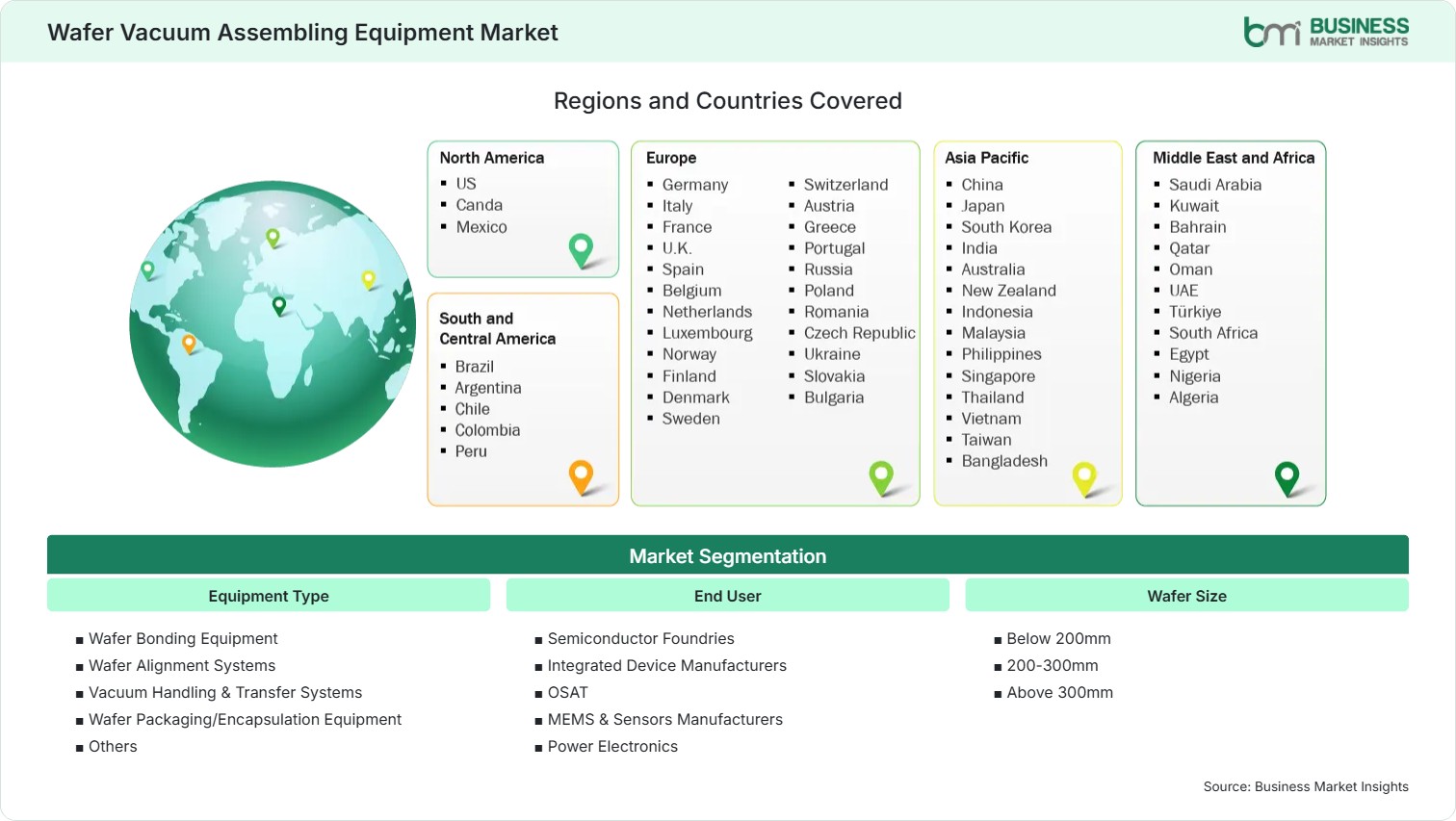
Global Market Geography
FREE PDF
Request your free sample
Request free sample
Segment Analysis

Wafer Vacuum Assembling Equipment Market Segmentation

Equipment Type

Wafer Bonding Equipment leads the structure with a 32%–36% share in 2025 and a 9.5%–10.4% CAGR through 2033. Demand reflects heterogeneous integration, MEMS fabrication, advanced packaging, and thin-wafer processing requirements.

  • Wafer Bonding Equipment: Facilitates the precise bonding of wafers to another wafer or to a substrate for MEMS, sensor applications, advanced packaging, and heterogeneous semiconductor integration.
  • Wafer Alignment Systems: Facilitates accurate positioning and alignment of wafers during assembly, which is essential for overlay control and bonding.
  • Vacuum Handling & Transfer Systems: Helps prevent contamination and damage to wafers through their handling in controlled transfer to/from processing and assembly stages.
  • Wafer Packaging/Encapsulation Equipment: Helps meet the needs of protective packaging and encapsulation of semiconductors, MEMS, sensors, and other electronic devices.

End User

Semiconductor Foundries represent a 30%–34% share in 2025 and are advancing at an 9.2%–10.1% CAGR, supported by outsourced manufacturing expansion, advanced packaging requirements, and increasing process complexity.

  • Semiconductor Foundries: Equipment requirements need to be flexible with high throughput for varied customers, wafers, packaging, and stringent process control standards.
  • Integrated Device Manufacturers (IDMs): Implement integrated equipment within internal manufacturing processes where process standardization, efficiency, automation, and equipment compatibility are essential.
  • OSAT: Precision assembly equipment can be used for outsourcing packaging needs like wafer handling, bonding, encapsulation, and advanced package development.
  • MEMS & Sensors Manufacturers: Require specialized bonding and alignment technologies for sensors, microstructures, and devices involving multiple materials and delicate wafer architectures.
  • Power Electronics: Uses controlled assembly processes for power semiconductor devices where thermal performance, structural reliability, and precise material integration influence product quality.

Wafer Size

The 200–300mm category holds a 55%–59% Wafer Vacuum Assembling Equipment Market share in 2025 and is advancing at a 9.0%–9.8% CAGR, supported by established semiconductor manufacturing infrastructure and broad equipment compatibility.

  • Below 200mm: Serves MEMS, sensors, specialty devices, research facilities, and mature semiconductor processes requiring flexible and specialized assembly capabilities.
  • 200–300mm: Supports mainstream semiconductor manufacturing through established fab infrastructure, mature automation, high-volume processing, and broad equipment availability.
  • Above 300mm: Addresses emerging high-throughput manufacturing requirements where larger substrates can improve production economics while demanding advanced handling and alignment precision.
Market Forces

Wafer Vacuum Assembling Equipment Market Dynamics

Key Market Drivers

Rising Semiconductor Production Drives Vacuum Assembly Demand

The increasing demands for semiconductor production are resulting in higher requirements for wafer handling, bonding, aligning, and packaging in controlled environments. With increasingly sophisticated architectures, it becomes important for the assembly equipment to be accurate and to reduce particle generation. The Wafer Vacuum Assembling Equipment Market growth opportunity, therefore, lies not only in handling but also in the provision of integrated equipment to perform several process steps. With increased automation in manufacturing, there comes the need for equipment that can work consistently through long cycles of production. The throughput rate, as well as the precision of alignment and vacuum control, together with other considerations, like maintenance and integration with manufacturing automation systems, is being taken into account by buyers. Machines that are capable of delivering a constant throughput with various types of wafers may become popular among those companies that wish to expand their production capacity. Such an atmosphere will benefit suppliers with solid process engineering capability.

Growing Wafer Fabrication Capacity Supports Equipment Adoption

New or expanding wafer production facilities will require large equipment infrastructure, thus providing room for assembly equipment systems that can be incorporated in automated production systems. Further increase in capacity has created additional demand for equipment systems that can accommodate wafers of different thicknesses and materials. Moreover, semiconductor companies are now looking for equipment systems that can adapt to future changes in the production process rather than those that will serve one single production process alone. The resultant buying pattern includes modularity, software, remote diagnosis, compatibility of the equipment, and after-sales service. Investment in advanced packaging facilities creates wider opportunities for the application base since wafer assembly ties front-end production with high-end back-end processes. Scalable equipment platforms from suppliers could be advantageous since fabs will require standard operating environments in their various production lines.

Increasing Need for Contamination Controlled Assembly Processes

With decreasing wafer size and increasingly complex device structures, contamination control will play an increasing role. The assembly machines have to be able to minimize particle production, create controlled environments, and handle wafer surfaces in order to prevent any contamination during the process. Such needs are driving the market towards vacuum-based handling and assembly systems, which decrease the exposure to contamination during key steps of the process. The Wafer Vacuum Assembling Equipment Market Trends include the tendency to implement automatic monitoring, material transportation, and process control into their equipment design. With the combination of vacuum and alignment, there would be reduced chances of creating defects due to poor handling. With this, manufacturers have begun considering contamination tolerance alongside production speed, size of equipment, and maintenance. It creates the possibility of developing more complex equipment that can work in clean production environments.

Key Market Opportunities

Expanding Semiconductor Manufacturing Creates New Opportunities

Global semiconductor manufacturing expansion is creating new opportunities for precision assembly equipment across foundries, IDMs, OSAT facilities, and specialty device manufacturers. Capacity additions require equipment that can support both established processes and emerging manufacturing architectures. Suppliers can capture value by developing configurable systems that accommodate multiple wafer dimensions, bonding techniques, and automation interfaces. Demand for localized semiconductor production is also broadening the geographical base for equipment procurement. The Wafer Vacuum Assembling Equipment Market forecast supports opportunities for suppliers that combine equipment sales with installation, process optimization, upgrades, and maintenance services. Long-term customer relationships can become particularly valuable where assembly systems are integrated deeply into production workflows. Vendors able to shorten installation periods and provide responsive technical support can strengthen their position in capacity-expansion projects.

Growing Investment in Advanced Wafer Fabrication Facilities

Investment in state-of-the-art wafer fabs is creating a demand for equipment that can facilitate increased precision and automation. State-of-the-art fabs present an opportunity for suppliers to create integrated handling, alignment, bonding, and monitoring systems rather than stand-alone machinery. High-level fabrication also makes equipment software a more critical issue because of the requirement for real-time monitoring, process traceability, and predictive maintenance in the production environment. Suppliers may differentiate themselves using modular platforms, which enable their customers to include additional functionality as needs arise. Research and pilot fabs also offer an opportunity because the equipment used at these sites may shape the specifications of the production line equipment in the future. Equipment manufacturers that have the capacity to support development as well as large-scale production will be able to create more robust business connections with customers.

Increasing Demand for High Precision Vacuum Equipment

The advanced requirements for wafer environmental control in processes like bonding, handling, encapsulation, and special assembly could provide an opportunity to the development of high-precision vacuum equipment. The possibility lies in the equipment that features automated wafer alignment, pressure control, contamination control, and process data acquisition. The semiconductor producers would be able to utilize such capabilities to increase the reproducibility of their production and minimize the need for manual intervention in the assembly process. There is also a growing demand from MEMS, sensors, power electronics, and other areas where material interface and structural precision impact device performance. Equipment producers have the chance to develop top-class positioning equipment through a combination of vacuum performance, smart process control, and flexible handling systems. Revenues from after-sales services, calibration, upgrade, and process optimization can be generated along with revenues from equipment sales, making the economic viability of an integrated system even stronger.

Market Restraints and Challenges

High Equipment Costs Limit Smaller Fabricator Adoption

Factor: Wafer assembly machines need a lot of money to be invested in precision mechanics, vacuum technologies, automation, controls, compatibility with clean manufacturing, and specific process capability. Impact: Significant initial investment may prevent small manufacturers, research companies, and specialty manufacturers with modest budgets from adopting wafer assembly machines. The customer could opt for machines that have the ability to be configured modularly or upgraded to lower the initial cost. The supplier may make the machines more accessible by means of leasing, maintenance contracts, refurbishing schemes, and configuring the equipment. Cost issues become significant when there is no sufficient volume of production to allocate equipment costs over it. Vendor systems that can prove to improve throughputs, yields, labor productivity, and process control are those that can make a better investment case for themselves.

Complex Maintenance Requirements Increase Operational Expenses

Factor: Vacuum pumps, precision alignment tools, sensors, automation systems, seals, chambers, and controls must be maintained and calibrated periodically. Impact: Difficulties in maintenance may result in higher operating costs and manufacturing risks if trained personnel and spare parts are not easily accessible. This is especially true in the case of high-volume semiconductor manufacturing operations, which require continuous operation of equipment. Hence, manufacturers are increasingly considering service support, spares availability, remote diagnostics, preventive maintenance, and training capabilities while making their supplier decisions. Condition monitoring, predictive maintenance, easy access to maintenance components, and standard replacement processes are ways to overcome this restriction for equipment designers.

Company Analysis

Competitive Landscape

The Wafer Vacuum Assembling Equipment Market analysis indicates competition among semiconductor equipment manufacturers, precision component specialists, vacuum technology providers, and integrated process-equipment suppliers. Competitive positioning centers on alignment precision, vacuum performance, automation, contamination control, equipment integration, service capability, and compatibility with advanced wafer-processing requirements.

Company Name

Overview

Products and Services relevant to this market

Shin-Etsu Chemical Co., Ltd.

Advanced materials company with semiconductor-related capabilities supporting demanding wafer-processing and electronic manufacturing applications.

Semiconductor materials, wafer-related products, processing materials, and technologies supporting controlled semiconductor manufacturing environments.

Nitto Denko Corporation

Diversified technology company providing advanced materials and processing solutions for electronics and semiconductor applications.

Semiconductor processing materials, wafer handling solutions, bonding materials, and precision electronic manufacturing technologies.

H-Square Corporation

Specialized provider of wafer handling and semiconductor manufacturing equipment serving precision wafer-processing applications.

Wafer handling equipment, wafer transfer systems, handling tools, and related semiconductor manufacturing solutions.

Ted Pella, Inc.

Supplies specialized laboratory and microscopy products alongside materials and tools used in semiconductor and research environments.

Wafer handling tools, cleanroom supplies, sample preparation products, and precision laboratory equipment.

SIPEL ELECTRONIC SA

Provides specialized electronic and semiconductor-related equipment and solutions for controlled manufacturing applications.

Semiconductor processing equipment, electronic manufacturing solutions, and specialized wafer-related technologies.

Hefei TREC Precision Equipment Co., Ltd.

Precision equipment manufacturer serving semiconductor and advanced electronics manufacturing applications.

Wafer handling, bonding, alignment, vacuum processing, and precision semiconductor equipment solutions.

Applied Materials, Inc.

Major semiconductor equipment supplier providing integrated manufacturing technologies for advanced device production.

Wafer processing, deposition, etch, inspection-related technologies, automation, and semiconductor manufacturing equipment.

Tokyo Electron Limited

Global semiconductor production equipment supplier with extensive capabilities across wafer-processing and manufacturing workflows.

Semiconductor processing equipment, wafer handling technologies, coating and developing systems, and integrated production solutions.

Lam Research Corporation

Semiconductor equipment provider focused on technologies supporting advanced wafer fabrication and device manufacturing.

Etch, deposition, wafer processing, cleaning, and integrated semiconductor manufacturing equipment and services.

KLA Corporation

Semiconductor technology company specializing in process control, inspection, and manufacturing intelligence.

Wafer inspection, metrology, process control, defect detection, and manufacturing analytics technologies.

Trust & Transparency

Research Methodology

The market analysis combines proprietary research with secondary data from government agencies, company disclosures, regulatory filings, industry databases and expert interviews. Market estimates are validated through data triangulation, cross-market benchmarking and analyst review.

View Full Research Methodology

Questions Answered

Frequently Asked Questions

What does the Wafer Vacuum Assembling Equipment Market report indicate about future competition?

The report indicates that competition will increasingly emphasize precision, automation, contamination control, modularity, software integration, service responsiveness, and compatibility with advanced wafer architectures. Suppliers capable of combining equipment performance with lifecycle support and adaptable process platforms should strengthen their competitive positioning.

Why is wafer bonding becoming important for semiconductor manufacturing?

Wafer bonding enables integration of different materials, device layers, and structures while supporting applications such as MEMS, sensors, advanced packaging, and heterogeneous semiconductor architectures. Precise bonding can facilitate compact device designs and support manufacturing approaches that require controlled interfaces between multiple wafer structures.

How is automation influencing wafer assembly equipment adoption?

Automation reduces manual wafer handling and supports consistent positioning, transfer, monitoring, and process execution. Automated systems can also improve traceability and reduce exposure to contamination. Integration with factory automation enables manufacturers to coordinate assembly equipment with broader production-management systems.

Which applications present the strongest opportunity in the market?

Wafer bonding, advanced packaging, MEMS fabrication, sensors, heterogeneous integration, and specialty semiconductor manufacturing offer strong opportunities. These applications require controlled wafer environments, precise alignment, repeatable bonding, and reliable handling, making them suitable for increasingly automated vacuum assembly platforms.

What factors are improving Wafer Vacuum Assembling Equipment Market return on investment?

Automation, improved alignment accuracy, contamination control, higher equipment utilization, reduced manual handling, and integration with semiconductor manufacturing workflows can improve equipment economics. Systems that support multiple process configurations and provide predictive maintenance capabilities can also extend useful equipment life and reduce unplanned downtime.

Access the Full Wafer Vacuum Assembling Equipment Market Report

Get segment-level forecasts, regional estimates, competitive benchmarking, company profiles and downloadable Excel datasets.

Access the full Wafer Vacuum Assembling Equipment Market Report
350 pages PDF & Excel | 2026-09-22
Similar Research

Related Market Reports