
3D IC Market Outlook: Size, Share, Trends, Growth Analysis, Competitive Landscape & Forecast, 2026–2033

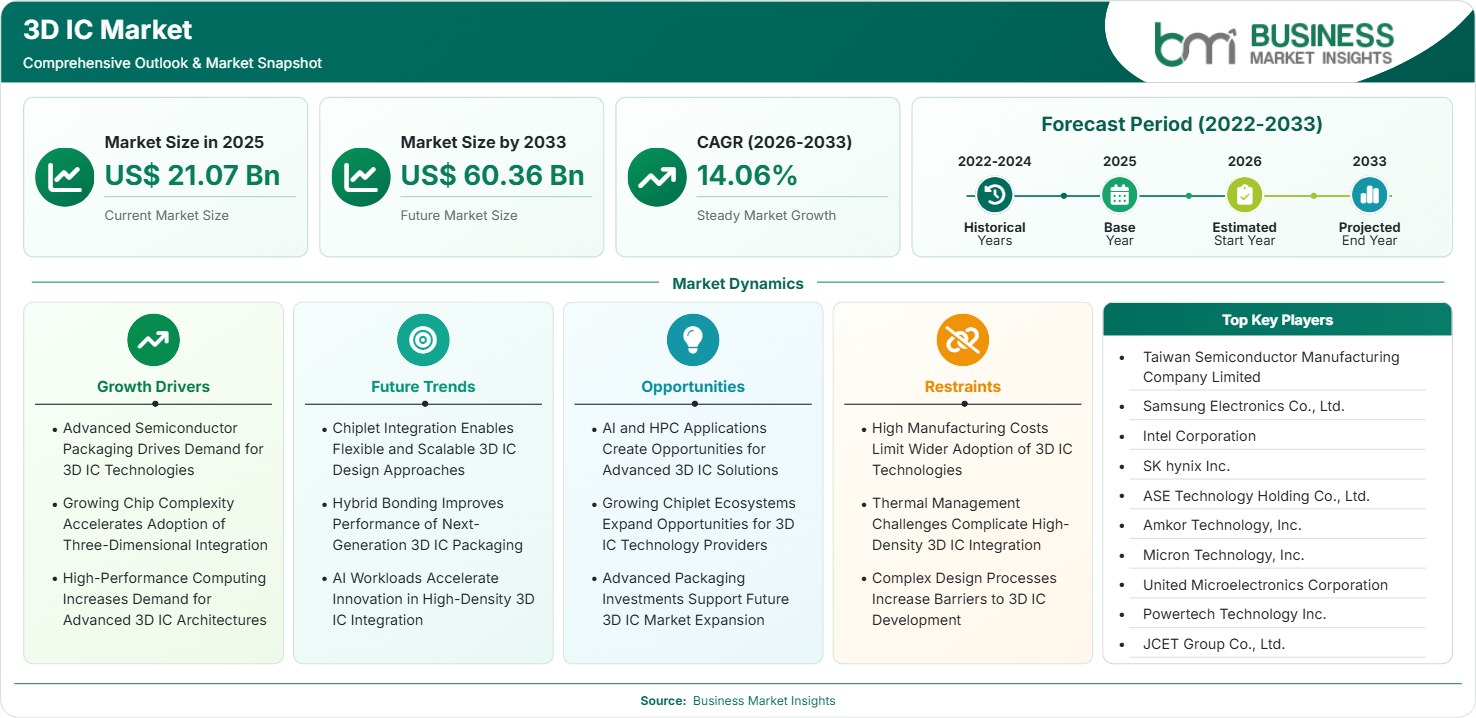
The 3D IC Market size was valued at US$ 21.07 Billion in 2025 and is projected to reach US$ 60.36 Billion by 2033, growing at a CAGR of 14.06% during 2026–2033, driven by advanced packaging, chip complexity, AI and HPC workloads, chiplet adoption, and continued semiconductor investment.

Report Coverage
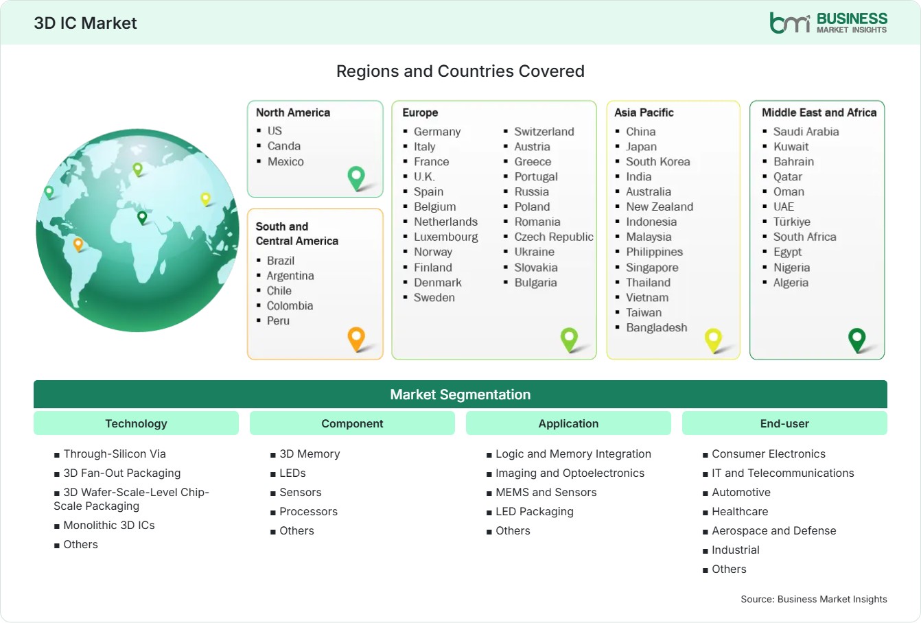
  • Technology: Through-Silicon Via , 3D Fan-Out Packaging, 3D Wafer-Scale-Level Chip-Scale Packaging , Monolithic 3D ICs, Others
  • Component: 3D Memory, LEDs, Sensors, Processors, Others
  • Application: Logic and Memory Integration, Imaging and Optoelectronics, MEMS and Sensors, LED Packaging, Others
  • End-user: Consumer Electronics, IT and Telecommunications, Automotive, Healthcare, Aerospace and Defense, Industrial, Others
US$ 21.07 Bn Market size in 2025
US$ 60.36 Bn Market Size by 2033
14.06% CAGR, 2026 - 2033
2026-2033 Forecast Period

AI Overview

3D IC Market Summary

  • North America Region: North America holds a share of 20%–24% in 2025, growing at a CAGR of 12%–14% during 2026–2033, supported by AI computing, advanced semiconductor design, defense electronics, and strong demand for high-performance computing architectures. The US market remains regionally dominant, with a CAGR of 12%–14% during 2026–2033, supported by AI accelerators, and demand for energy-efficient computing.
  • Fastest Growing Region: Asia Pacific holds a share of 58%–63% in 2025 and is projected to grow at a CAGR of 15%–17% through 2033, supported by semiconductor manufacturing concentration, advanced packaging capacity, memory production, AI infrastructure investment, chiplet adoption, and expanding electronics production ecosystems.
  • Leading Segment: Through-Silicon Via (TSV) holds a share of 38%–43% in 2025 and is projected to grow at a CAGR of 13%–15% through 2033, supported by high-bandwidth memory, vertical integration, advanced processors, shorter interconnects, improved bandwidth, and growing demand for high-performance computing architectures.
  • High Growth Segment: Processors represent a share of 28%–33% in 2025 and are projected to grow at a CAGR of 16%–18% through 2033, driven by AI accelerators, data center workloads, chiplet architectures, advanced computing requirements, and increasing demand for greater performance within constrained power envelopes.
  • Key Market Opportunity: AI accelerators, high-bandwidth memory, chiplet-based architectures, advanced packaging investments, and heterogeneous integration create significant opportunities for semiconductor manufacturers, foundries, outsourced assembly providers, and specialized packaging technology developers.
  • Major Market Players: Taiwan Semiconductor Manufacturing Company Limited, Samsung Electronics Co., Ltd., Intel Corporation, SK hynix Inc., ASE Technology Holding Co., Ltd., Amkor Technology, Inc., Micron Technology, Inc., United Microelectronics Corporation, Powertech Technology Inc., JCET Group Co., Ltd.
Strategic Insights

3D IC Market: Strategic Insights

3D IC Market Strategic Framework
FREE PDF
Request your free sample
Request free sample
Stakeholder View

Key Takeaways

  • The value chain is becoming more integrated as foundries, IDMs, OSAT companies, memory manufacturers, EDA providers, and semiconductor designers collaborate to address increasingly complex packaging requirements.
  • AI and high-performance computing provide the strongest near-term growth opportunity, particularly for processor integration, high-bandwidth memory, and architectures requiring high data throughput with reduced interconnect distances.
  • Hybrid bonding, TSV-based stacking, wafer-level processes, and chiplet architectures are becoming important innovation pathways as semiconductor companies seek higher performance without relying exclusively on conventional transistor scaling.
  • Asia Pacific offers the strongest investment case due to its concentration of semiconductor manufacturing, memory production, foundry capacity, advanced packaging facilities, and electronics supply chains.
  • Capital expenditure is increasingly directed toward advanced packaging facilities, equipment, and process development as semiconductor manufacturers seek greater control over complex heterogeneous integration technologies.
  • Thermal management is becoming a critical design consideration, creating opportunities for advanced cooling materials, thermal interface technologies, package-level heat dissipation, and design optimization solutions.
Geographic Outlook

3D IC Market Regional Highlights

North America 3D IC Market

North America held a 3D IC Market share of 20%–24% in 2025 and is projected to grow at a CAGR of 12%–14% through 2033. The US represents the region's dominant market, supported by semiconductor design leadership, AI infrastructure investment, defense electronics, and advanced packaging initiatives.

  • US semiconductor investments are supporting advanced packaging development as companies seek greater domestic capabilities for AI processors, memory integration, and high-performance computing components.
  • AI infrastructure expansion is increasing demand for advanced processors and memory architectures capable of handling large-scale workloads with greater bandwidth and improved energy efficiency.
  • Defense and aerospace applications create demand for specialized semiconductor packaging where performance, reliability, miniaturization, and secure domestic supply chains are strategically important.
  • Leading technology companies are investing in chiplet-based architectures to improve design flexibility, accelerate product development, and combine specialized processing functions within advanced packages.

US 3D Ic Market

The US accounted for 78%–82% of North America's 3D Ic Market share in 2025 and is projected to grow at a CAGR of 12%–14% through 2033. The country benefits from leading semiconductor design capabilities, major AI technology investments, advanced processor development, and government support for domestic semiconductor manufacturing.

  • Domestic semiconductor initiatives are encouraging investment in fabrication and advanced packaging infrastructure, strengthening opportunities across the US semiconductor ecosystem.
  • AI accelerators and high-performance computing processors are increasing demand for advanced packaging solutions that provide greater bandwidth and improved power efficiency.
  • Chiplet architectures are gaining importance as semiconductor designers seek modular development approaches that can combine different process nodes and specialized functions.

Europe 3D Ic Market

Europe represented a 3D Ic Market share of 8%–11% in 2025 and is projected to grow at a CAGR of 10%–12% through 2033. Germany and France are leading regional markets, while the Netherlands provides strong semiconductor ecosystem support through equipment and technology capabilities. Germany is projected to grow at a CAGR of 11%–13%, while France is expected to expand at 10%–12%.

  • Germany remains a leading opportunity because of its automotive semiconductor ecosystem, industrial manufacturing base, and increasing investment in advanced electronics and semiconductor technologies.
  • France benefits from aerospace, defense, industrial, and electronics applications requiring compact, reliable, and high-performance semiconductor solutions.
  • The Netherlands contributes critical semiconductor equipment capabilities, supporting the broader European ecosystem for advanced manufacturing and packaging technologies.
  • European semiconductor initiatives are encouraging greater investment in domestic production capabilities and reducing strategic dependence on external semiconductor supply chains.

Asia Pacific 3D Ic Market

Asia Pacific held a 3D Ic Market share of 58%–63% in 2025 and is projected to grow at a CAGR of 15%–17% through 2033. Taiwan, South Korea, Japan, and China represent major regional markets supported by foundries, memory manufacturers, semiconductor assembly capabilities, and electronics production. China is projected to experience a CAGR of 16%–18%, supported by domestic semiconductor investment and growing demand for advanced computing technologies.

  • Taiwan remains a leading market due to its concentration of advanced foundry manufacturing, semiconductor design ecosystems, and sophisticated packaging capabilities.
  • South Korea benefits from strong memory production and semiconductor manufacturing expertise, supporting demand for vertically integrated memory and advanced packaging technologies.
  • China is expanding domestic semiconductor capabilities and investing in advanced packaging to improve supply chain resilience and support AI and computing applications.
  • Japan contributes through semiconductor materials, equipment, electronics manufacturing, and specialized technologies supporting advanced packaging development.

Rest of World 3D Ic Market

South and Central America represented a 2%–3% share of the 3D Ic Market in 2025 and are projected to grow at a CAGR of 9%–11%. Brazil and Mexico provide leading regional opportunities due to electronics manufacturing, automotive production, and growing technology investments. Mexico benefits from proximity to North American supply chains and expanding electronics manufacturing activity. Regional adoption remains smaller than Asia Pacific, but demand for advanced electronics creates opportunities for specialized semiconductor applications. The Middle East and Africa accounted for a 2%–4% share in 2025 and are projected to grow at a CAGR of 11%–13%. The UAE, Saudi Arabia, and Israel represent important technology markets, supported by AI investment, semiconductor research, defense electronics, and digital infrastructure.

  • Mexico is benefiting from electronics and automotive manufacturing investments, creating opportunities for advanced semiconductor components and packaging technologies within regional supply chains.
  • Brazil represents the largest electronics market in South America, supporting demand for semiconductor components used in consumer and industrial applications.
  • Israel offers strong opportunities through semiconductor design, AI technology, defense electronics, and advanced computing research capabilities.
  • The UAE and Saudi Arabia are investing heavily in AI and digital infrastructure, increasing long-term demand for high-performance computing and advanced semiconductor systems.
  • Regional semiconductor ecosystems remain comparatively smaller, creating opportunities for specialized applications, technology partnerships, and localized electronics manufacturing investments.
Global Market Geography
FREE PDF
Request your free sample
Request free sample
Segment Analysis

3D IC Market Segmentation

Technology

Through-Silicon Via (TSV) represented a 38%–43% share in 2025 and is projected to grow at a CAGR of 13%–15% through 2033. The technology supports high-bandwidth vertical interconnections and remains important for stacked memory and advanced processor architectures.

  • Through-Silicon Via (TSV): TSV enables vertical electrical connections through silicon, supporting high bandwidth, shorter interconnects, and efficient stacking for memory and high-performance computing applications.
  • 3D Fan-Out Packaging: Fan-out packaging improves integration density without conventional substrate constraints, supporting compact devices, heterogeneous integration, and performance-focused applications across consumer and computing electronics.
  • 3D Wafer-Scale-Level Chip-Scale Packaging (WLCSP): Wafer-level chip-scale packaging supports compact semiconductor footprints, efficient manufacturing, and integration requirements for sensors, mobile devices, and miniaturized electronics.
  • Monolithic 3D ICs: Monolithic integration enables vertically stacked device layers within a single silicon structure, potentially improving density and interconnect efficiency for advanced computing architectures.
  • Others: Emerging hybrid bonding and advanced stacking approaches complement established integration methods, supporting specialized applications requiring greater bandwidth, compact dimensions, and improved system-level performance.

Component

Processors represented a 28%–33% share in 2025 and are projected to grow at a CAGR of 16%–18% through 2033. AI and HPC workloads are increasing demand for compact, high-performance processor architectures with improved bandwidth and energy efficiency.

  • 3D Memory: Stacked memory improves bandwidth and reduces interconnect distances, supporting AI accelerators, data centers, high-performance computing, and increasingly demanding data-intensive workloads.
  • LEDs: Advanced three-dimensional packaging can improve integration and compactness for LED applications, supporting display technologies, lighting systems, automotive electronics, and specialized optoelectronic products.
  • Sensors: Three-dimensional integration enables compact sensor architectures combining sensing, processing, and communication functions for automotive, healthcare, industrial, and consumer electronics applications.
  • Processors: Advanced 3D integration improves computing density and connectivity, supporting AI accelerators, high-performance processors, data center workloads, and energy-efficient heterogeneous computing architectures.
  • Others: Specialized components benefit from advanced integration where compact dimensions, higher functionality, and improved electrical performance are required across emerging semiconductor applications.

Application

Logic and Memory Integration represented a 42%–47% share in 2025 and is projected to grow at a CAGR of 15%–17% through 2033. Growing AI and data-intensive workloads are increasing demand for integrated architectures that improve data movement efficiency.

  • Logic and Memory Integration: Combining logic and memory improves data access efficiency and bandwidth, supporting AI computing, high-performance processors, data centers, and advanced consumer electronics.
  • Imaging and Optoelectronics: Three-dimensional integration supports compact imaging and optical systems by combining sensors, processing, and photonic components within increasingly space-constrained device architectures.
  • MEMS and Sensors: Advanced packaging enables compact integration of MEMS devices, sensors, processing elements, and communication functions for automotive, healthcare, industrial, and consumer applications.
  • LED Packaging: Advanced packaging improves LED integration, thermal performance, and compactness, supporting displays, automotive lighting, consumer electronics, and specialized illumination systems.
  • Others: Emerging applications use 3D integration to achieve greater functionality, miniaturization, and performance across specialized electronics requiring advanced semiconductor packaging approaches.

End-user

IT and Telecommunications represented a 31%–36% share in 2025 and is projected to grow at a CAGR of 15%–17% through 2033. Data center expansion, AI infrastructure, networking equipment, and high-performance computing are increasing demand for advanced semiconductor integration.

  • Consumer Electronics: Compact devices increasingly require high-performance processors, memory, sensors, and advanced packaging to deliver greater functionality within smaller physical footprints.
  • IT and Telecommunications: Data centers, AI infrastructure, networking systems, and high-performance computing require advanced semiconductor architectures delivering greater bandwidth, performance, and energy efficiency.
  • Automotive: Advanced driver assistance, autonomous driving, electrification, and connected vehicles are increasing demand for compact, high-performance semiconductor systems and sensor integration.
  • Healthcare: Medical imaging, wearable devices, diagnostics, and monitoring equipment benefit from miniaturized semiconductor systems combining sensors, processing, and communication capabilities.
  • Aerospace and Defense: Mission-critical applications require high-performance, compact, and reliable semiconductor architectures supporting advanced sensing, communications, computing, and electronic warfare systems.
  • Industrial: Automation, robotics, machine vision, and industrial IoT applications require integrated semiconductor solutions supporting real-time processing, sensing, connectivity, and energy efficiency.
  • Others: Emerging applications across specialized electronics are adopting advanced packaging where compact form factors, high performance, and heterogeneous integration provide clear system-level benefits.
Market Forces

3D IC Market Dynamics

Key Market Drivers

Advanced Semiconductor Packaging Drives Demand for 3D IC Technologies

Advanced semiconductor packaging is becoming a critical pathway for improving performance as conventional scaling encounters increasing technical and economic challenges. 3D integration enables semiconductor manufacturers to combine multiple dies, memory layers, and processing components within compact packages, improving bandwidth and reducing interconnect distances. Demand is particularly strong in AI accelerators, high-performance computing, and advanced memory applications where conventional two-dimensional packaging can create bandwidth and power constraints. The resulting 3D IC Market growth is supported by the need to deliver higher computing performance without proportional increases in physical footprint or energy consumption.

Growing Chip Complexity Accelerates Adoption of Three-Dimensional Integration

Increasing semiconductor complexity is encouraging manufacturers to move beyond traditional monolithic designs and adopt heterogeneous integration approaches. Modern processors increasingly combine computing cores, memory, input-output functions, accelerators, and specialized processing units, creating challenges related to interconnect density and power efficiency. Three-dimensional integration can address these challenges by placing functional components closer together and enabling greater system-level integration. Chiplet architectures are reinforcing this trend by allowing semiconductor designers to combine dies produced using different process technologies.

High-Performance Computing Increases Demand for Advanced 3D IC Architectures

High-performance computing and AI workloads require increasingly large volumes of data to move rapidly between processors and memory. Conventional packaging approaches can create bottlenecks because long interconnects consume energy and limit bandwidth. 3D architectures address these challenges by enabling closer integration between computing and memory components, supporting higher bandwidth and lower communication latency. The resulting 3D IC Market trends include greater adoption of stacked memory, chiplets, hybrid bonding, and heterogeneous integration. Semiconductor manufacturers are prioritizing packaging innovations that can improve performance per watt and support increasingly demanding computational workloads.

Key Market Opportunities

AI and HPC Applications Create Opportunities for Advanced 3D IC Solutions

AI and high-performance computing represent some of the strongest opportunities for advanced 3D integration because these workloads require exceptional computing throughput, memory bandwidth, and energy efficiency. AI accelerators increasingly depend on high-bandwidth memory and advanced packaging to move large datasets between processing and memory components efficiently. Semiconductor companies can capture growth by developing architectures that integrate processors, memory, and specialized accelerators within compact packages. The expansion of AI infrastructure is encouraging substantial investment in semiconductor manufacturing and packaging capacity, creating opportunities for foundries, OSAT providers, equipment manufacturers.

Growing Chiplet Ecosystems Expand Opportunities for 3D IC Technology Providers

Chiplet architecture is presenting new business opportunities for firms that offer technologies capable of helping achieve the goal of achieving modular semiconductor integration. By using chiplets, it becomes possible to combine different chips in one chip package and thus achieve more flexible design possibilities without the requirement for manufacturing all functionalities on the best process node. Such an approach makes it possible to create chips that would have computing, memory, networking, and accelerator functions. The evolving chiplet ecosystem has created demand for standards for advanced interconnection, packaging, testing, thermal management, and design technologies.

Advanced Packaging Investments Support Future 3D IC Market Expansion

Advanced packaging investments are expanding as semiconductor manufacturers recognize that packaging technology is becoming as strategically important as transistor scaling. Leading foundries, memory manufacturers, integrated device manufacturers, and OSAT providers are increasing investments in advanced packaging capacity to address demand from AI, automotive, telecommunications, and high-performance computing. These investments are creating opportunities across equipment, materials, process engineering, testing, and packaging services. The long-term 3D IC Market Forecasts are therefore supported by sustained investment in packaging infrastructure and the need for higher-performance semiconductor systems.

Market Restraints and Challenges

High Manufacturing Costs Limit Wider Adoption of 3D IC Technologies

Factor: 3D IC manufacturing requires specialized equipment, advanced packaging processes, complex wafer handling, precision alignment, extensive testing, and high capital expenditure, resulting in greater production costs than conventional packaging approaches. Impact: High manufacturing costs can restrict adoption to applications where performance improvements justify additional expenses, limiting broader deployment in cost-sensitive consumer and industrial electronics. Yield management is another concern because defects in stacked dies or complex interconnections can reduce overall package reliability and increase manufacturing losses.

Thermal Management Challenges Complicate High-Density 3D IC Integration

Factor: High power densities from vertically packaged semiconductor devices create localized heat generation within small packaging, increasing the difficulty of dissipating heat as computing density grows and energy usage increases. Impact: Thermal considerations could affect achievable performance, cooling needs, and packaging, especially for AI accelerators and high-performance computing. The usual cooling technologies might be inadequate when several powerful semiconductor devices are packaged close together.

Company Analysis

Competitive Landscape

3D Ic Market analysis indicates that competition is concentrated among semiconductor foundries, integrated device manufacturers, memory producers, OSAT providers, and specialized packaging companies. Competitive differentiation is increasingly based on advanced packaging capacity, TSV expertise, hybrid bonding capabilities, memory integration, chiplet support, manufacturing yield, and ability to serve AI and high-performance computing customers.

Company Name

Overview

Products and Services relevant to this market

Taiwan Semiconductor Manufacturing Company Limited

Leading semiconductor foundry with extensive capabilities in advanced process technologies and sophisticated semiconductor packaging.

3D IC technologies, advanced packaging, 3DFabric, chiplet integration, CoWoS, InFO, and wafer-level integration services.

Samsung Electronics Co., Ltd.

Global semiconductor manufacturer with strong capabilities across memory, logic, foundry, and advanced packaging technologies.

3D IC integration, HBM, advanced packaging, chiplet technologies, semiconductor manufacturing, and memory solutions.

Intel Corporation

Integrated semiconductor company developing advanced processors, packaging technologies, chiplets, and heterogeneous integration architectures.

3D packaging, Foveros, EMIB, chiplet integration, advanced processors, and high-performance computing solutions.

SK hynix Inc.

Major memory semiconductor manufacturer with strong expertise in high-bandwidth memory and advanced memory packaging.

3D stacked memory, HBM, advanced packaging, memory integration, and high-performance semiconductor solutions.

ASE Technology Holding Co., Ltd.

Leading semiconductor packaging and testing provider serving global semiconductor manufacturers and system companies.

Advanced packaging, 3D IC assembly, wafer-level packaging, testing, system-in-package, and heterogeneous integration services.

Amkor Technology, Inc.

Global outsourced semiconductor packaging and test provider supporting advanced semiconductor integration and packaging requirements.

Advanced 3D packaging, wafer-level packaging, system-in-package, flip-chip, testing, and semiconductor assembly services.

Micron Technology, Inc.

Global memory and storage semiconductor company developing advanced memory technologies for computing and data-intensive applications.

3D NAND, HBM, advanced memory packaging, high-performance memory, and semiconductor integration technologies.

United Microelectronics Corporation

Global semiconductor foundry providing specialized manufacturing capabilities across multiple process technologies and applications.

Specialty semiconductor manufacturing, advanced packaging support, wafer fabrication, and integrated circuit production services.

Powertech Technology Inc.

Semiconductor assembly and testing company with strong capabilities in memory packaging and advanced semiconductor manufacturing services.

Memory packaging, 3D stacked packaging, semiconductor assembly, testing, and advanced packaging services.

JCET Group Co., Ltd.

Major semiconductor packaging and testing provider offering advanced integration capabilities for global semiconductor customers.

3D IC packaging, wafer-level packaging, system-in-package, chiplet integration, assembly, and semiconductor testing.

Trust & Transparency

Research Methodology

The market analysis combines proprietary research with secondary data from government agencies, company disclosures, regulatory filings, industry databases and expert interviews. Market estimates are validated through data triangulation, cross-market benchmarking and analyst review.

View Full Research Methodology

Questions Answered

Frequently Asked Questions

Which applications offer the strongest opportunities?

AI accelerators, high-performance computing, high-bandwidth memory, advanced processors, and data center infrastructure offer strong growth opportunities.

What is the main challenge in the market?

Thermal management is a major challenge because vertically stacked components concentrate heat within increasingly dense semiconductor packages.

Why are chiplets important for 3D ICs?

Chiplets enable modular integration of specialized dies, improving design flexibility and supporting complex heterogeneous semiconductor architectures.

Which region leads the 3D IC market report?

Asia Pacific leads due to its concentration of foundries, memory manufacturers, OSAT providers, and electronics production ecosystems.

What is driving 3D IC adoption?

AI computing, high-performance processors, advanced memory, chiplet integration, and increasing semiconductor complexity are accelerating adoption.

Access the Full 3D IC Market Report

Get segment-level forecasts, regional estimates, competitive benchmarking, company profiles and downloadable Excel datasets.

Access the full 3D IC Market Report
350 pages PDF & Excel | 2026-08-31
Similar Research

Related Market Reports