
Wafer Inspection Equipment Market Outlook: Size, Share, Trends, Growth Analysis, Competitive Landscape & Forecast, 2026-2033

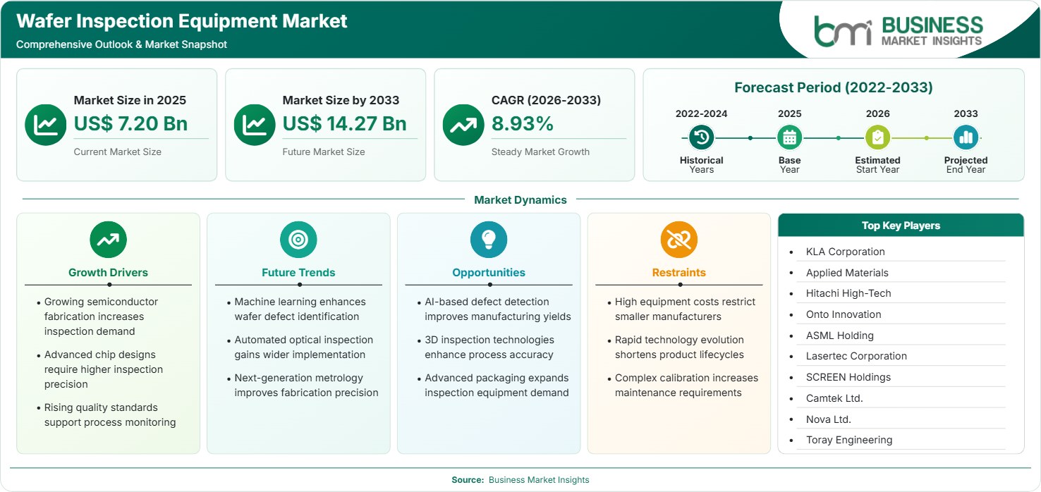
The Wafer Inspection Equipment Market size was valued at US$ 7.20 billion in 2025 and is projected to reach US$ 14.27 billion by 2033, growing at a CAGR of 8.93% during 2026–2033. Growing semiconductor fabrication capacity, rising demand for advanced process control, and increasing investments in defect inspection technologies continue creating strong opportunities for equipment manufacturers.

Report Coverage
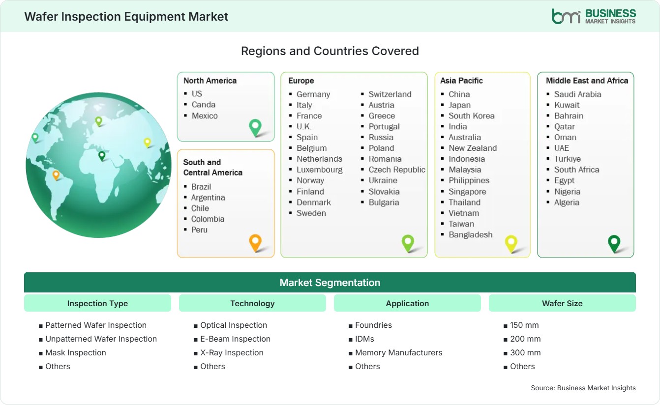
  • Inspection Type: Patterned Wafer Inspection, Unpatterned Wafer Inspection, Mask Inspection, Others
  • Technology: Optical Inspection, E-Beam Inspection, X-Ray Inspection, Others
  • Application: Foundries, IDMs, Memory Manufacturers, Others
  • Wafer Size: 150 mm, 200 mm, 300 mm, Others
US$ 7.20 Bn Market size in 2025
US$ 14.27 Bn Market Size by 2033
8.93% CAGR, 2026 - 2033
2026-2033 Forecast Period

AI Overview

Wafer Inspection Equipment Market Summary

  • North America Region: North America holds 29%–32% market share in 2025 and is projected to expand at a CAGR of 8.4%–8.9% during 2026–2033. Strong semiconductor investments, advanced research capabilities, and domestic chip manufacturing initiatives continue supporting market expansion. The U.S. remains the regional leader, recording a CAGR of 8.5%–9.0%, supported by fab expansion, government incentives, and process control innovation.
  • Fastest Growing Region: Asia Pacific accounts for 48%–51% market share in 2025 and is expected to register a CAGR of 9.6%–10.2%, supported by expanding foundry capacity, increasing memory production, and continuous investments in semiconductor manufacturing technologies.
  • Leading Segment: Patterned Wafer Inspection captures 37%–40% market share in 2025 and is anticipated to grow at a CAGR of 9.0%–9.5%, driven by increasing process complexity and advanced node manufacturing.
  • High Growth Segment: Optical Inspection represents 41%–44% market share in 2025 and is projected to record a CAGR of 9.4%–9.9%, supported by faster throughput, higher inspection accuracy, and broad adoption in semiconductor fabrication facilities.
  • Key Market Opportunity: Increasing adoption of AI-powered inspection systems, advanced packaging technologies, and automated defect classification continues creating significant growth opportunities for semiconductor equipment manufacturers.
  • Major Market Players: KLA Corporation, Applied Materials, Inc., Hitachi High-Tech Corporation, Onto Innovation Inc., ASML Holding N.V., Lasertec Corporation, SCREEN Holdings Co., Ltd., Camtek Ltd., Nova Ltd., and Toray Engineering Co., Ltd.
Strategic Insights

Wafer Inspection Equipment Market: Strategic Insights

Wafer Inspection Equipment Market Strategic Framework
FREE PDF
Request your free sample
Request free sample
Stakeholder View

Key Takeaways

  • Semiconductor manufacturers continue prioritizing advanced inspection technologies to improve production yields, reduce defect rates, and enhance overall manufacturing efficiency at increasingly smaller process nodes.
  • AI-enabled defect detection platforms are becoming essential for reducing inspection time while improving classification accuracy across complex semiconductor manufacturing environments.
  • Foundries and integrated device manufacturers remain the primary customers, driven by continuous investments in next-generation semiconductor fabrication facilities.
  • Asia Pacific provides the strongest long-term investment opportunity through rapid fab construction, government incentives, and expanding semiconductor production ecosystems.
  • Strategic partnerships between inspection equipment suppliers and semiconductor manufacturers are accelerating commercialization of next-generation process control technologies.
  • Investments in advanced packaging inspection, 3D metrology, and high-resolution optical systems continue strengthening competitive differentiation among leading market participants.
Geographic Outlook

Wafer Inspection Equipment Market Regional Highlights

North America Wafer Inspection Equipment Market

North America accounts for 29%–32% Wafer Inspection Equipment Market share in 2025 and is expected to register a CAGR of 8.4%–8.9% during 2026–2033. Regional demand is supported by government semiconductor incentives, advanced research infrastructure, and continued investments in wafer fabrication facilities. Equipment suppliers are introducing high-resolution inspection platforms to support advanced logic, memory, and specialty semiconductor manufacturing while improving production yields and operational efficiency.

  • Government semiconductor funding continues supporting domestic wafer fabrication expansion and advanced manufacturing capabilities.
  • AI processor development increases demand for high-precision inspection technologies capable of detecting nanoscale defects.
  • Research institutions collaborate with equipment suppliers to accelerate inspection technology innovation.
  • Semiconductor manufacturers continue modernizing fabrication facilities with automated inspection and process control systems.

US Wafer Inspection Equipment Market

The United States contributes 83%–86% of North American revenue and is projected to expand at a CAGR of 8.5%–9.0% during the forecast period. Increasing investments in domestic semiconductor manufacturing, technology innovation, and advanced research continue strengthening long-term equipment demand.

  • Large semiconductor manufacturers continue expanding wafer fabrication capacity across multiple U.S. states.
  • Federal semiconductor initiatives encourage investments in advanced inspection technologies.
  • Growing AI chip production increases demand for sophisticated process monitoring equipment.
  • Equipment suppliers continue investing in next-generation optical and e-beam inspection platforms.

Europe Wafer Inspection Equipment Market

Europe represents 18%–21% market share in 2025 and is projected to grow at a CAGR of 8.1%–8.6% through 2026–2033. Semiconductor manufacturing expansion, automotive electronics production, and public investments supporting regional chip manufacturing continue driving inspection equipment demand. Germany remains the leading regional market, while Ireland records the fastest growth due to expanding semiconductor manufacturing investments.

  • European semiconductor initiatives encourage investment in advanced manufacturing equipment.
  • Automotive semiconductor demand supports inspection technology adoption across fabrication facilities.
  • Equipment suppliers continue developing higher-resolution optical inspection systems.
  • Increasing research collaboration strengthens semiconductor process innovation throughout the region.

Asia Pacific Wafer Inspection Equipment Market

Asia Pacific holds 48%–51% market share in 2025 and is projected to register the fastest 9.6%–10.2% CAGR during the forecast period. China, Taiwan, South Korea, and Japan continue expanding semiconductor fabrication capacity while increasing investments in advanced process technologies. China remains the largest regional market, whereas India demonstrates the fastest growth owing to expanding semiconductor manufacturing initiatives and policy support.

  • Foundry expansion significantly increases demand for wafer inspection and process control systems.
  • Memory manufacturers continue investing in advanced inspection technologies for higher production yields.
  • Government incentives support semiconductor ecosystem development across multiple Asian economies.
  • Equipment suppliers strengthen regional manufacturing and technical support capabilities.

Rest of World Wafer Inspection Equipment Market

The Rest of World region accounts for 4%–7% market share in 2025 and is expected to expand at a CAGR of 8.3%–8.8% during 2026–2033. Growth is supported by emerging semiconductor investments, electronics manufacturing expansion, and increasing adoption of advanced inspection equipment across developing markets in Latin America and the Middle East.

  • Israel continues expanding semiconductor research and specialty chip manufacturing capabilities.
  • Brazil strengthens electronics manufacturing, supporting gradual inspection equipment demand.
  • Middle Eastern technology investments encourage semiconductor ecosystem development.
  • Growing industrial digitalization supports demand for semiconductor production infrastructure.
Global Market Geography
FREE PDF
Request your free sample
Request free sample
Segment Analysis

Wafer Inspection Equipment Market Segmentation

Inspection Type

Inspection type remains the foundation of semiconductor process control as manufacturers require different inspection methods throughout wafer fabrication. This segment accounted for 37%–40% market share in 2025 and is projected to register a CAGR of 9.0%–9.5% during 2026–2033. Increasing manufacturing complexity, shrinking semiconductor geometries, and stricter yield targets continue expanding the Wafer Inspection Equipment Market scope, encouraging fabs to deploy highly specialized inspection systems across multiple production stages.

  • Patterned Wafer Inspection: Represents the largest sub-segment owing to increasing inspection requirements at advanced technology nodes where complex circuit patterns require highly accurate defect identification during semiconductor manufacturing.
  • Unpatterned Wafer Inspection: Widely adopted for monitoring raw wafer quality, identifying substrate defects, and ensuring contamination-free surfaces before lithography and other critical fabrication processes begin.
  • Mask Inspection: Plays a vital role in detecting defects on photomasks used during lithography, helping manufacturers maintain pattern accuracy and reduce production losses across advanced semiconductor fabrication.

Technology

Technology selection significantly influences inspection speed, defect sensitivity, and production efficiency across semiconductor manufacturing facilities. The segment captured 41%–44% market share in 2025 and is anticipated to expand at a CAGR of 9.4%–9.9% through the forecast period. Current Wafer Inspection Equipment Market trends indicate increasing adoption of AI-enabled inspection platforms, high-resolution imaging systems, and hybrid technologies capable of supporting next-generation semiconductor production.

  • Optical Inspection: Dominates the technology landscape because of its high throughput, non-contact operation, cost efficiency, and ability to inspect large wafer volumes during semiconductor manufacturing.
  • E-Beam Inspection: Provides extremely high-resolution imaging for detecting nanoscale defects that cannot be identified using conventional optical inspection technologies, particularly at advanced process nodes.
  • X-Ray Inspection: Supports non-destructive inspection of semiconductor structures, advanced packaging, and multilayer devices by identifying hidden internal defects without damaging wafer integrity.

Application

Application diversity continues expanding as semiconductor manufacturers increase investments in advanced logic, memory, and specialty chip production. This segment accounted for 45%–48% market share in 2025 and is expected to register a CAGR of 9.2%–9.7% during 2026–2033. Inspection equipment remains essential for maintaining production yields, improving process stability, and minimizing manufacturing defects throughout wafer fabrication facilities.

  • Foundries: Represent the largest application due to high-volume semiconductor manufacturing, continuous process optimization, and increasing investments in advanced fabrication technologies supporting global chip demand.
  • IDMs: Utilize sophisticated inspection systems throughout integrated manufacturing operations to improve product quality, optimize production efficiency, and support advanced semiconductor technology development.
  • Memory Manufacturers: Continue investing in high-resolution inspection equipment to improve yields, detect nanoscale defects, and maintain manufacturing consistency across DRAM, NAND flash, and emerging memory technologies.

Wafer Size

Wafer size directly influences production efficiency, equipment utilization, and semiconductor manufacturing economics. This segment held 63%–66% market share in 2025 and is projected to grow at a CAGR of 9.1%–9.6% through 2026–2033. Growing investments in larger wafer processing technologies continue increasing demand for advanced inspection platforms capable of supporting higher throughput and greater inspection precision.

  • 150 mm: Continues serving mature semiconductor production, power electronics, analog devices, sensors, and specialty applications requiring reliable inspection solutions for established manufacturing processes.
  • 200 mm: Maintains steady demand across automotive semiconductors, industrial electronics, MEMS devices, and power management chips where production expansion supports continued inspection equipment deployment.
  • 300 mm: Accounts for the largest share owing to widespread adoption in advanced logic, memory, artificial intelligence processors, and high-performance computing semiconductor manufacturing requiring state-of-the-art inspection technologies.
Market Forces

Wafer Inspection Equipment Market Dynamics

Key Market Drivers

Growing semiconductor fabrication increases inspection demand

Semiconductor manufacturing capacities all around the globe keep growing due to increased requirements for AI chips, automobiles electronics, computers and advanced consumer electronics. Every single new facility needs advanced inspection systems which would be able to detect even nanoscale defects on wafers. Companies are actively investing in advanced process control systems which will improve manufacturing yields and reduce expensive wafer losses. Incentive programs for semiconductors in the USA, Europe, Japan, South Korea, and India are making fab construction and equipment purchase faster. These developments continue strengthening Wafer Inspection Equipment Market growth, creating sustained demand for high-precision inspection platforms across advanced semiconductor manufacturing facilities.

Advanced chip designs require higher inspection precision

The transition toward smaller process nodes, chiplet architectures, and increasingly complex semiconductor designs is significantly increasing inspection requirements. High-end integrated circuits consist of billions of transistors having very small features, which necessitate high levels of precision in defect identification during production. Optical and electron beam inspection technologies keep on developing in order to achieve higher image resolutions, better sensitivity and increased speed without decreasing efficiency in manufacturing process. Nowadays semiconductor manufacturers use AI-based defect identification software in order to improve accuracy of classification and reduce number of false alarms.

Rising quality standards support process monitoring

Semiconductor companies are continuously improving their quality control measures in order to increase their wafer yields and lower variability in their fabrication process. With the help of current inspection equipment, the processes such as lithography, etching, deposition, and packaging can be continuously monitored, helping engineers detect any deviations in the processes before there is any loss from the manufacturing process. The current need for reliable semiconductor products in the automotive, aerospace, automation, and medical electronics industries is driving more improvements in the process monitoring technology. These developments remain central to Wafer Inspection Equipment Market trends worldwide.

Key Market Opportunities

AI-based defect detection improves manufacturing yields

Artificial intelligence is transforming semiconductor inspection by enabling automated defect classification, real-time analytics, and predictive process optimization. AI algorithms significantly reduce manual inspection workloads while improving defect recognition accuracy across increasingly complex semiconductor designs. Equipment manufacturers continue integrating machine learning into inspection platforms to accelerate production and improve yield management. Wafer Inspection Equipment Market Forecasts indicate that AI-enabled inspection solutions will become a primary competitive differentiator as semiconductor manufacturers prioritize automation, higher throughput, and lower manufacturing costs across advanced fabrication facilities.

3D inspection technologies enhance process accuracy

Three-dimensional inspection technologies are becoming increasingly important for advanced semiconductor manufacturing because they provide precise measurement of wafer topography, multilayer structures, and complex device geometries. High-resolution 3D metrology improves detection of surface irregularities and dimensional variations that conventional two-dimensional inspection systems may overlook. Equipment suppliers continue introducing faster scanning technologies and enhanced imaging capabilities to support advanced packaging, heterogeneous integration, and next-generation semiconductor architectures. Growing investment in three-dimensional inspection is expected to strengthen long-term market opportunities for leading equipment manufacturers.

Advanced packaging expands inspection equipment demand

Rapid adoption of advanced semiconductor packaging technologies, including chiplets, fan-out wafer-level packaging, and 3D integration, is increasing demand for sophisticated inspection equipment. These packaging methods require highly accurate inspection throughout multiple manufacturing stages to ensure interconnect reliability and structural integrity. Equipment manufacturers are developing inspection systems capable of identifying defects within increasingly complex package architectures while maintaining production efficiency. Continued expansion of advanced packaging for artificial intelligence processors, data centers, automotive electronics, and high-performance computing applications is expected to support sustained equipment demand.

Market Restraints and Challenges

High equipment costs restrict smaller manufacturers

Advanced wafer inspection systems require substantial investment because they combine sophisticated optics, electron beam technologies, artificial intelligence software, and precision automation. Factor: High acquisition, installation, calibration, and maintenance costs create significant financial barriers for smaller semiconductor manufacturers and emerging fabrication facilities. Impact: Limited capital availability may delay equipment upgrades, reduce adoption of next-generation inspection technologies, and widen the technology gap between large integrated manufacturers and smaller industry participants, particularly in developing semiconductor markets.

Rapid technology evolution shortens product lifecycles

The semiconductor industry evolves rapidly as manufacturing processes transition toward increasingly smaller process nodes and more complex chip architectures. Factor: Continuous technological advancement requires equipment manufacturers to accelerate research, development, and product upgrades to remain competitive. Impact: Shorter equipment lifecycles increase development costs, accelerate product obsolescence, and require semiconductor manufacturers to make frequent capital investments in advanced inspection platforms, creating financial and operational challenges across the semiconductor manufacturing value chain.

Company Analysis

Competitive Landscape

Competition is centered on inspection accuracy, artificial intelligence integration, high-throughput imaging, and support for advanced semiconductor process nodes. Wafer Inspection Equipment Market analysis indicates that leading manufacturers are investing heavily in optical metrology, e-beam inspection, defect classification software, and advanced packaging inspection platforms. Strategic partnerships with foundries and integrated device manufacturers continue strengthening technology leadership and expanding global service capabilities.

Company Name

Overview

Products and Services Relevant to this Market

KLA Corporation

Global leader in semiconductor process control and yield management solutions serving advanced chip manufacturers worldwide.

Wafer inspection systems, defect review equipment, process control software, metrology solutions, reticle inspection, and yield management platforms.

Applied Materials, Inc.

Leading semiconductor equipment manufacturer providing fabrication technologies for advanced integrated circuit production.

Wafer inspection equipment, process diagnostics, semiconductor manufacturing systems, AI-enabled inspection software, and process control technologies.

Hitachi High-Tech Corporation

Develops advanced analytical and inspection equipment supporting semiconductor fabrication and quality assurance.

Electron beam inspection systems, defect review equipment, metrology solutions, analytical instruments, and semiconductor inspection technologies.

Onto Innovation Inc.

Specializes in process control, optical metrology, and advanced inspection solutions for semiconductor manufacturers.

Optical inspection systems, 3D metrology, process control software, advanced packaging inspection, and defect analysis solutions.

ASML Holding N.V.

Global semiconductor equipment company supporting advanced lithography and integrated process control solutions.

Semiconductor inspection technologies, computational lithography solutions, process optimization software, and advanced manufacturing support systems.

Lasertec Corporation

Japanese manufacturer specializing in high-resolution inspection equipment for semiconductor fabrication processes.

Mask inspection systems, wafer inspection platforms, laser-based inspection technologies, and advanced semiconductor quality control equipment.

SCREEN Holdings Co., Ltd.

Provides semiconductor production equipment supporting inspection, cleaning, and process optimization applications.

Optical wafer inspection systems, semiconductor cleaning equipment, inspection software, and production automation technologies.

Camtek Ltd.

Develops inspection and metrology systems for semiconductor manufacturing and advanced packaging applications.

Wafer inspection equipment, advanced packaging inspection systems, metrology solutions, defect analysis software, and automated quality control platforms.

Nova Ltd.

Supplies metrology and process control technologies for advanced semiconductor manufacturing facilities worldwide.

Optical metrology systems, chemical process monitoring, wafer measurement technologies, AI-driven analytics, and process control solutions.

Toray Engineering Co., Ltd.

Manufactures precision inspection equipment supporting semiconductor fabrication and electronic component production.

Wafer inspection systems, semiconductor manufacturing equipment, precision measurement technologies, automated inspection platforms, and quality assurance systems.

Trust & Transparency

Research Methodology

The market analysis combines proprietary research with secondary data from government agencies, company disclosures, regulatory filings, industry databases and expert interviews. Market estimates are validated through data triangulation, cross-market benchmarking and analyst review.

View Full Research Methodology

Questions Answered

Frequently Asked Questions

What does the Wafer Inspection Equipment Market Report cover?

The Market Report provides detailed insights into market dynamics, technology developments, regional performance, competitive landscape, segmentation analysis, investment opportunities, emerging applications, and long-term industry outlook.

Which region is expected to register the fastest growth?

Asia Pacific is projected to record the fastest growth due to rapid semiconductor fabrication expansion, government incentives, increasing foundry investments, and strong demand for advanced logic and memory manufacturing technologies.

Why is AI becoming important in wafer inspection?

Artificial intelligence improves automated defect classification, reduces false detections, accelerates inspection workflows, and enables predictive process optimization, allowing semiconductor manufacturers to achieve higher production yields and improved operational efficiency.

Which inspection technology leads the market?

Optical inspection remains the leading technology because it provides high throughput, excellent defect detection capability, non-contact inspection, and cost-effective monitoring across high-volume semiconductor manufacturing operations.

What is driving demand for wafer inspection equipment?

Increasing semiconductor fabrication capacity, growing adoption of artificial intelligence chips, advanced packaging technologies, and stricter quality requirements are driving sustained demand for high-precision wafer inspection systems.

Access the Full Wafer Inspection Equipment Market Report

Get segment-level forecasts, regional estimates, competitive benchmarking, company profiles and downloadable Excel datasets.

Access the full Wafer Inspection Equipment Market Report
350 pages PDF & Excel | 2026-08-24