
Semiconductor Metrology and Inspection Equipment Market Outlook: Size, Share, Trends, Growth Analysis, Competitive Landscape & Forecast, 2026-2033

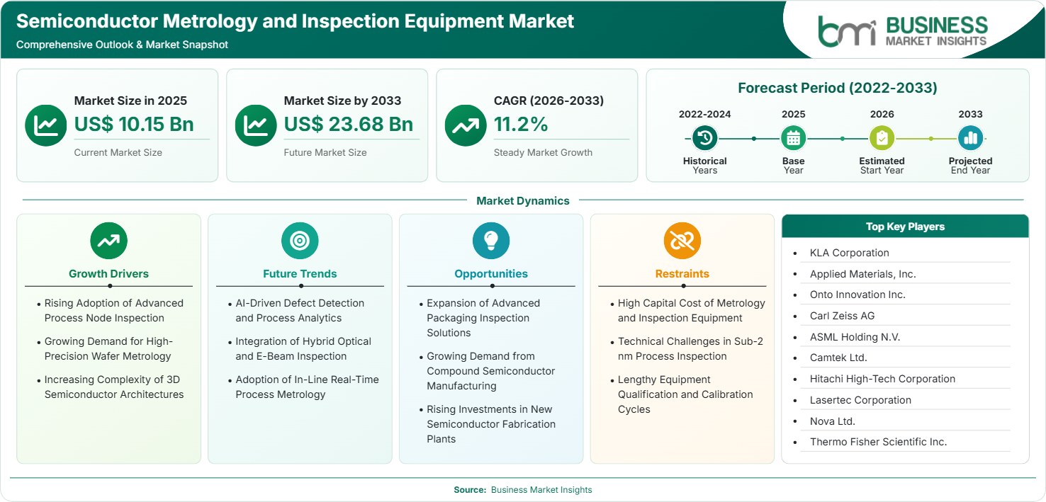
The Semiconductor Metrology & Inspection Equipment Market size was valued at US$ 10.15 Billion in 2025 and is projected to reach US$ 23.68 Billion by 2033, growing at a CAGR of 11.2% during 2026–2033. Growth is supported by rising semiconductor complexity, increasing adoption of advanced process nodes, growing demand for AI and high-performance computing chips, and expanding investments in wafer fabrication facilities globally.

Report Coverage
  • Type: Optical, Beam
  • Technology: Wafer Inspection System, Mask Inspection System, Thin Film Metrology, Package Inspection, Others
  • Dimension: 2D Metrology/Inspection, 3D Metrology/Inspection, Hybrid 2D/3D Systems
  • End-User: Foundries, Integrated Device Manufacturing Firms, Outsourced Semiconductor Assembly and Test Companies, Others
US$ 10.15 Bn Market size in 2025
US$ 23.68 Bn Market Size by 2033
11.2% CAGR, 2026 - 2033
2026-2033 Forecast Period

01 AI Overview

Semiconductor Metrology and Inspection Equipment Market Summary

  • North America Region: North America holds a market share of 30%–33% in 2025, growing at a CAGR of 10.2%–11.0% during 2026–2033. Strong semiconductor R&D activity, advanced fabrication capabilities, and increasing investments in AI-driven chip production continue supporting market growth. The U.S. remains the largest regional market, expanding at a CAGR of 10.5%–11.3%.
  • Fastest Growing Region: Asia Pacific accounts for 39%–42% of revenue in 2025 and is projected to grow at a CAGR of 12.0%–12.8% through 2033. Expanding foundry capacity, high semiconductor production volumes, and government-backed chip manufacturing initiatives drive adoption.
  • Leading Segment: Optical systems hold a market share of 62%–66% in 2025 and are expected to expand at a CAGR of 10.8%–11.6%. Their ability to provide high-throughput inspection and defect detection across advanced semiconductor manufacturing processes supports segment leadership.
  • High Growth Segment: Wafer Inspection System accounts for 34%–38% of revenue in 2025 and is projected to register a CAGR of 11.8%–12.6% during the forecast period. Increasing process complexity and shrinking node sizes continue fueling demand.
  • Key Market Opportunity: Growing deployment of advanced packaging, chiplet architectures, and sub-3nm semiconductor manufacturing processes is creating significant opportunities for next-generation metrology and inspection technologies.
  • Major Market Players: KLA Corporation, Applied Materials, Inc., Onto Innovation Inc., Carl Zeiss AG, ASML Holding N.V., Camtek Ltd., Hitachi High-Tech Corporation, Lasertec Corporation, Nova Ltd., and Thermo Fisher Scientific Inc.
02 Strategic Insights

Semiconductor Metrology and Inspection Equipment Market: Strategic Insights

Semiconductor Metrology and Inspection Equipment Market Strategic Framework
FREE PDF
Request your free sample
Request free sample
03 Stakeholder View

Key Takeaways

  • The market ecosystem is closely integrated with wafer fabrication equipment suppliers, semiconductor foundries, integrated device manufacturers, packaging firms, and advanced materials providers.
  • Wafer inspection remains the most attractive growth opportunity due to increasing defect density challenges associated with advanced process nodes and high-volume manufacturing.
  • Innovation is increasingly centered on AI-driven defect classification, high-resolution e-beam inspection, hybrid metrology systems, and in-line process control solutions.
  • Asia Pacific continues to offer the strongest investment potential because of expanding foundry ecosystems, capacity additions, and government-supported semiconductor manufacturing programs.
  • The major semiconductor metrology & inspection equipment market trend includes strategic partnerships between inspection equipment providers and semiconductor manufacturers as process complexity rises across advanced nodes
  • Advanced packaging technologies, including heterogeneous integration and chiplet-based architectures, are expanding the importance of inspection and metrology throughout semiconductor production workflows.
04 Geographic Outlook

Semiconductor Metrology and Inspection Equipment Market Regional Highlights

North America Semiconductor Metrology & Inspection Equipment Market

North America accounted for 30%–33% of global revenue in 2025 and is projected to expand at a CAGR of 10.2%–11.0% through 2033. The region benefits from strong semiconductor R&D capabilities, advanced process development activities, and significant investments in domestic chip manufacturing. Semiconductor Metrology & Inspection Equipment Market share leadership is reinforced by the presence of major equipment providers, advanced logic production facilities, and increasing government support for semiconductor self-sufficiency initiatives.

  • Advanced-node semiconductor manufacturing continues increasing demand for high-resolution inspection and metrology platforms capable of detecting nanoscale defects.
  • Semiconductor producers are investing heavily in process control systems to improve yield rates and reduce manufacturing variability.
  • Growth in AI, data center, and automotive semiconductor production is expanding requirements for sophisticated inspection technologies.
  • Government-backed semiconductor manufacturing programs continue supporting equipment procurement and technology upgrades.
  • Equipment suppliers are focusing on AI-enabled analytics and automated defect classification capabilities to enhance operational efficiency.

US Semiconductor Metrology & Inspection Equipment Market

The United States represented 26%–29% of global revenue in 2025 and is anticipated to register a CAGR of 10.5%–11.3% during the forecast period. Demand is supported by increasing capital expenditure in advanced semiconductor fabrication, strong research activity, and expansion of domestic manufacturing capacity. Continued growth in AI chips, high-performance computing devices, and defense-related semiconductor technologies contributes to sustained Semiconductor Metrology & Inspection Equipment Market growth.

  • Investments in next-generation semiconductor fabs are increasing purchases of wafer inspection and metrology equipment.
  • Advanced logic and memory chip production require increasingly sophisticated defect detection and process control systems.
  • AI accelerator and data center processor demand continues driving equipment upgrades throughout manufacturing facilities.
  • Strong collaboration between equipment suppliers and semiconductor producers supports ongoing technological advancement.

Europe Semiconductor Metrology & Inspection Equipment Market

Europe accounted for 20%–23% of global revenue in 2025 and is projected to grow at a CAGR of 10.8%–11.6% through 2033. Growth is supported by investments in semiconductor sovereignty, automotive electronics production, and advanced research initiatives. Germany remains the leading market with a CAGR of 10.9%–11.7%, while Ireland emerges as the fastest-growing market at a CAGR of 11.8%–12.6%, driven by expanding semiconductor manufacturing investments.

  • European semiconductor initiatives are increasing demand for advanced metrology and inspection systems.
  • Automotive electronics and industrial semiconductor applications continue supporting equipment purchases.
  • Germany benefits from strong semiconductor research capabilities and established industrial manufacturing ecosystems.
  • Ireland is witnessing rising investment in semiconductor manufacturing and advanced technology infrastructure.
  • Increasing adoption of advanced packaging technologies is creating additional demand for high-precision inspection solutions.

Asia Pacific Semiconductor Metrology & Inspection Equipment Market

Asia Pacific held 39%–42% of global revenue in 2025 and is expected to remain the fastest-growing region, expanding at a CAGR of 12.0%–12.8% through 2033. The region benefits from extensive semiconductor manufacturing capacity, strong foundry ecosystems, and significant government support for domestic chip production. China remains the largest market with a CAGR of 11.8%–12.6%, while India records the highest growth at 12.8%–13.6%.

  • Foundries continue expanding advanced-node production capacity, increasing demand for sophisticated inspection equipment.
  • China is investing heavily in semiconductor manufacturing capabilities and process control technologies.
  • India is attracting semiconductor investments through policy support and manufacturing incentive programs.
  • Advanced packaging, heterogeneous integration, and chiplet architectures are increasing metrology requirements.
  • Rising demand for consumer electronics and AI chips continues supporting regional semiconductor production expansion.

Rest of World Semiconductor Metrology & Inspection Equipment Market

The Rest of World region represented 7%–9% of global revenue in 2025 and is projected to expand at a CAGR of 10.5%–11.3% through 2033. Growth is supported by emerging semiconductor investments, increasing electronics manufacturing activity, and diversification of global semiconductor supply chains.

Brazil is the leading semiconductor metrology & inspection equipment market in South & Central America and is expected to grow at a CAGR of 10.7%–11.5%. In the Middle East & Africa, the United Arab Emirates is projected to be the fastest-growing country, registering a CAGR of 11.0%–11.8% through the forecast period.

  • Electronics manufacturing expansion is creating demand for semiconductor process control technologies.
  • Governments are pursuing semiconductor ecosystem development to strengthen technology capabilities.
  • Brazil continues investing in electronics and advanced manufacturing sectors.
  • The United Arab Emirates is increasing investments in technology infrastructure and innovation-driven industries.
  • Supply chain diversification initiatives are encouraging new semiconductor investments across emerging markets.
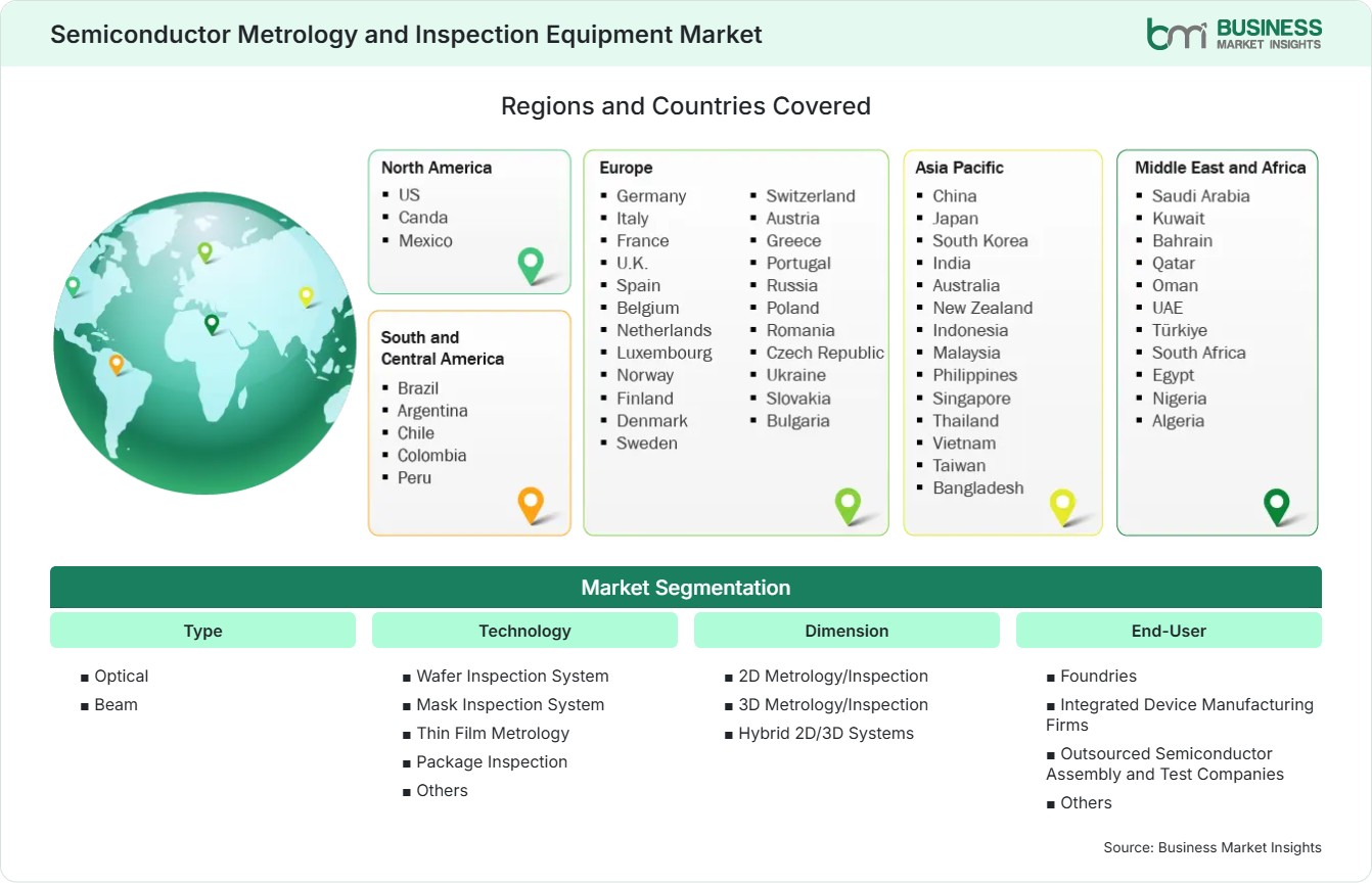
Global Market Geography
FREE PDF
Request your free sample
Request free sample
05 Segment Analysis

Semiconductor Metrology and Inspection Equipment Market Segmentation

Type

Type remains a fundamental classification within the semiconductor metrology & inspection equipment market forecast, influencing inspection speed, resolution capability, and process control performance. This segment accounted for approximately 62%–66% market share in 2025 and is projected to expand at a CAGR of 10.8%–11.6% through 2033. Increasing complexity of semiconductor manufacturing processes is driving demand for advanced inspection technologies capable of identifying nanoscale defects and process variations with high accuracy.

  • Optical: Optical systems dominate the market due to their high throughput, broad inspection coverage, and suitability for advanced wafer manufacturing environments.
  • Beam: Beam-based systems are increasingly utilized in advanced process nodes where superior defect sensitivity and nanoscale inspection precision are required.

Technology

Technology advancements continue shaping equipment demand across semiconductor manufacturing facilities. This segment accounted for approximately 34%–38% market share in 2025 and is expected to register a CAGR of 11.8%–12.6% through 2033. The market scope continues expanding as fabrication facilities intensify investments in process control and yield management technologies.

  • Wafer Inspection System: High demand stems from the need to detect pattern defects, contamination, and process variations throughout semiconductor production.
  • Mask Inspection System: Mask inspection systems support lithography accuracy by identifying defects on photomasks before production deployment.
  • Thin Film Metrology: These solutions provide precise measurement of film thickness, composition, and critical dimensions essential to advanced processes.
  • Package Inspection: Increasing adoption of advanced packaging technologies is driving demand for sophisticated package-level inspection systems.

Dimension

Dimension-based inspection is becoming increasingly important as semiconductor structures become more complex and vertically integrated. This segment accounted for approximately 29%–33% market revenue in 2025 and is projected to grow at a CAGR of 11.5%–12.3% during the forecast period. Manufacturers increasingly require multidimensional measurement capabilities to maintain process accuracy.

  • 2D Metrology/Inspection: Widely used for surface inspection, dimensional verification, and defect detection across conventional manufacturing processes.
  • 3D Metrology/Inspection: Growing adoption is driven by advanced packaging, FinFET structures, and complex semiconductor architectures requiring depth analysis.
  • Hybrid 2D/3D Systems: Hybrid platforms provide comprehensive process monitoring by combining two-dimensional and three-dimensional measurement capabilities.

End-User

End-user demand is driven by increasing investments in advanced semiconductor manufacturing, packaging technologies, and process node development. This segment accounted for approximately 48%–52% market share in 2025 and is forecast to expand at a CAGR of 11.0%–11.8% through 2033. The Semiconductor Metrology & Inspection Equipment Market share is heavily influenced by capital expenditure trends across semiconductor production ecosystems.

  • Foundries: Foundries represent the largest customer group due to their extensive investments in process control and yield optimization technologies.
  • Integrated Device Manufacturing (IDM) Firms: IDMs continue deploying advanced inspection systems to enhance production efficiency and maintain quality standards.
  • Outsourced Semiconductor Assembly and Test (OSAT) Companies: OSAT providers increasingly require inspection technologies to support advanced packaging and testing processes.
06 Market Forces

Semiconductor Metrology and Inspection Equipment Market Dynamics

Key Market Drivers

Rising Adoption of Advanced Process Node Inspection

The semiconductor industry is moving quickly into the manufacturing nodes that involve continuous reductions of the features to below those found in prior technology nodes. This brings a high probability of having losses due to minute defects or variations during production. This, therefore, necessitates the need to use advanced inspection tools that can detect defects at minute sizes. There is also continued growth in advanced process node development for AI processors, high-performance computing, and advanced memory technologies, hence driving strong demand for semiconductor metrology & inspection equipment market.

Growing Demand for High-Precision Wafer Metrology

Precision metrology has become essential for maintaining process control throughout semiconductor manufacturing operations. As device architectures become more sophisticated, manufacturers require highly accurate measurements of critical dimensions, overlay accuracy, film thickness, and surface characteristics. Advanced wafer metrology systems help improve production consistency, reduce defects, and maximize yield performance. Increasing investments in leading-edge semiconductor fabrication facilities are creating sustained demand for equipment capable of delivering precise measurements while supporting high-volume manufacturing requirements. These requirements continue strengthening the role of metrology solutions within modern chip production environments.

Increasing Complexity of 3D Semiconductor Architectures

The adoption of 3D NAND, FinFETs, gate-all-around transistors, and advanced packaging structures is increasing manufacturing complexity across the semiconductor industry. These architectures require highly sophisticated inspection and measurement capabilities that extend beyond traditional two-dimensional analysis techniques. Manufacturers must accurately characterize multilayer structures, complex geometries, and densely integrated components throughout production. Growing utilization of 3D chip architectures across memory, logic, and AI applications continues accelerating investments in advanced metrology and inspection solutions capable of supporting next-generation semiconductor technologies.

Key Market Opportunities

Expansion of Advanced Packaging Inspection Solutions

Advanced packaging technologies are becoming increasingly important for achieving higher performance, lower power consumption, and greater integration density. Techniques such as heterogeneous integration, chiplets, and 3D stacking require enhanced inspection and metrology capabilities throughout packaging processes. As semiconductor manufacturers pursue more sophisticated packaging strategies, demand is expected to increase for specialized inspection systems capable of ensuring reliability, alignment accuracy, and manufacturing quality. Equipment providers offering advanced packaging inspection solutions are likely to benefit from these evolving industry requirements.

Growing Demand from Compound Semiconductor Manufacturing

The increasing adoption of compound semiconductors in electric vehicles, telecommunications infrastructure, renewable energy systems, and industrial electronics is creating attractive opportunities for equipment suppliers. Materials such as silicon carbide and gallium nitride require specialized inspection and metrology approaches due to their unique material characteristics and manufacturing processes. As production capacity expands across compound semiconductor markets, investment in advanced process control technologies is expected to increase correspondingly, creating additional demand for specialized inspection platforms.

Rising Investments in New Semiconductor Fabrication Plants

Governments and semiconductor companies worldwide are investing billions of dollars in new fabrication facilities to strengthen supply chains and enhance manufacturing capacity. Every new fabrication plant requires extensive deployment of inspection and metrology equipment to support process development, production optimization, and quality assurance activities. Growing capital expenditure across foundries, memory manufacturers, and integrated device manufacturers is expected to generate significant opportunities for semiconductor metrology & inspection equipment market throughout the forecast period. Long-term fab construction pipelines continue supporting strong market fundamentals.

Market Restraints and Challenges

High Capital Cost of Metrology and Inspection Equipment

Factor: Advanced metrology and inspection systems incorporate highly sophisticated optics, sensors, software algorithms, and precision engineering components that significantly increase equipment costs.

Impact: High acquisition and maintenance expenses can create barriers for smaller semiconductor manufacturers and emerging production facilities. Capital-intensive purchasing requirements often extend procurement cycles and limit technology adoption among budget-constrained organizations. Elevated equipment costs can also influence return-on-investment calculations and affect purchasing decisions during periods of market uncertainty.

Technical Challenges in Sub-2 nm Process Inspection

Factor: Ongoing semiconductor miniaturization is pushing manufacturing processes toward dimensions where defect detection and measurement become increasingly difficult.

Impact: Inspection accuracy, defect sensitivity, throughput optimization, and data analysis complexity become more challenging as process nodes advance. Equipment suppliers must continuously develop new technologies capable of maintaining measurement precision while supporting high-volume manufacturing. These technical challenges contribute to increased development costs and complexity across next-generation inspection platforms.

07 Company Analysis

Competitive Landscape

The market is highly consolidated and technology-intensive, with leading companies focusing on optical inspection, e-beam systems, advanced metrology platforms, AI-powered defect analysis, and process control solutions. Semiconductor Metrology & Inspection Equipment Market analysis indicates that innovation, resolution capability, throughput performance, and support for advanced process nodes remain key competitive differentiators.

Company Name

Overview

Products and Services Relevant to this Market

KLA Corporation

Global leader in semiconductor process control and yield management technologies.

Wafer inspection, reticle inspection, metrology systems, process analytics solutions.

Applied Materials, Inc.

Major semiconductor equipment provider serving advanced fabrication facilities worldwide.

Inspection systems, process control solutions, metrology technologies, semiconductor equipment.

Onto Innovation Inc.

Specialized provider of process control and advanced inspection technologies.

Metrology equipment, inspection systems, yield optimization solutions.

Carl Zeiss AG

Precision optics and imaging technology company serving semiconductor manufacturing.

Optical metrology systems, advanced imaging solutions, semiconductor optics technologies.

ASML Holding N.V.

Leading lithography and semiconductor equipment manufacturer.

Metrology solutions, process control technologies, semiconductor manufacturing systems.

Camtek Ltd.

Inspection and metrology equipment provider focused on advanced semiconductor applications.

Wafer inspection, advanced packaging inspection, process control equipment.

Hitachi High-Tech Corporation

Technology company delivering semiconductor inspection and measurement tools.

Critical dimension SEM systems, defect review systems, metrology solutions.

Lasertec Corporation

Specialist in inspection technologies for semiconductor manufacturing.

Mask inspection systems, wafer inspection equipment, process monitoring solutions.

Nova Ltd.

Provider of advanced metrology systems supporting semiconductor fabrication.

Optical metrology solutions, process control platforms, dimensional measurement systems.

Thermo Fisher Scientific Inc.

Advanced analytical instrumentation provider serving semiconductor industries.

Electron microscopy systems, materials characterization solutions, inspection technologies.

08 Industry Activity

Recent Developments

May 2026

KLA Corporation expanded advanced wafer inspection capabilities focused on supporting next-generation semiconductor process nodes and AI-driven manufacturing environments.

May 2026

Merck announced the opening of a €20 million Metrology & Inspection site in Saint‑Ismier, France, expanding production capacity for semiconductor inspection tools fivefold to support advanced chip manufacturing, AI-driven applications, and Europe’s semiconductor ecosystem.

February 2026

Siemens announced the acquisition of Canopus AI to enhance its semiconductor manufacturing portfolio with AI-driven metrology and inspection solutions, strengthening its electronic design automation (EDA) capabilities and enabling more precise wafer and mask inspection for advanced chip manufacturing.

February 2026

Applied Materials, Inc. introduced enhanced process control technologies designed to improve yield management across advanced logic and memory semiconductor production.

10 Trust & Transparency

Research Methodology

The market analysis combines proprietary research with secondary data from government agencies, company disclosures, regulatory filings, industry databases and expert interviews. Market estimates are validated through data triangulation, cross-market benchmarking and analyst review.

View Full Research Methodology

11 Questions Answered

Frequently Asked Questions

What is the main challenge for equipment manufacturers?

Maintaining inspection accuracy and throughput at increasingly advanced process nodes while controlling equipment complexity and costs remains a major challenge.

Which end-user segment represents the largest demand?

Foundries represent the largest end-user segment because of extensive investments in advanced-node manufacturing and process control infrastructure.

Why is wafer inspection the leading technology segment?

Wafer inspection is critical for identifying manufacturing defects early in production, helping manufacturers improve yield and reduce costly process losses.

Which type dominates the semiconductor metrology & inspection equipment market report?

Optical inspection and metrology systems dominate due to their high throughput, broad process coverage, and effectiveness in large-scale manufacturing environments.

What is semiconductor metrology and inspection equipment used for?

These systems are used to detect defects, measure critical dimensions, monitor process variations, and improve manufacturing yield throughout semiconductor production.

Access the Full Semiconductor Metrology and Inspection Equipment Market Report

Get segment-level forecasts, regional estimates, competitive benchmarking, company profiles and downloadable Excel datasets.

Access the full Semiconductor Metrology and Inspection Equipment Market Report
350 pages PDF & Excel | 2026-07-30