
Semiconductor Defect Inspection Equipment Market Size, Share, Trends & Forecast Report, 2026–2033

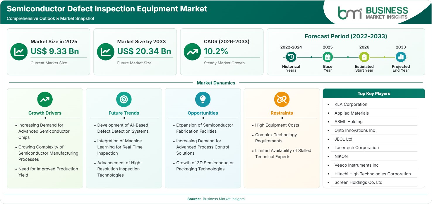
The Semiconductor Defect Inspection Equipment Market size was valued at US$ 9.33 billion in 2025 and is projected to reach US$ 20.34 billion by 2033, growing at a CAGR of US$ 10.2% during 2026–2033, driven by advanced semiconductor manufacturing, increasing chip complexity, artificial intelligence applications, and demand for higher production yields.

Report Coverage
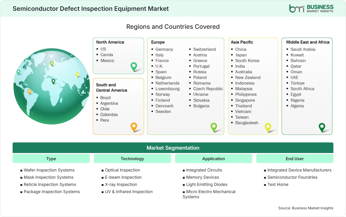
  • Type: Wafer Inspection Systems, Mask Inspection Systems, Reticle Inspection Systems, Package Inspection Systems
  • Technology: Optical Inspection, E-beam Inspection, X-ray Inspection, UV & Infrared Inspection
  • Application: Integrated Circuits, Memory Devices, Light Emitting Diodes, Micro Electro Mechanical Systems
  • End User: Integrated Device Manufacturers, Semiconductor Foundries, Test Home
US$ 9.33 Bn Market size in 2025
US$ 20.34 Bn Market Size by 2033
10.2% CAGR, 2026 - 2033
2026-2033 Forecast Period

01 AI Overview

Semiconductor Defect Inspection Equipment Market Summary

  • North America Region: North America holds a 32%–35% share in 2025, growing with a CAGR of 9%–11% influenced by semiconductor investments, fabrication expansion, advanced process control adoption, and government incentives. The US market advances with a CAGR of 10%–12% due to domestic semiconductor capacity development.
  • Fastest Growing Region: Asia Pacific captures a 38%–41% share in 2025 and records a CAGR of 11%–13% supported by semiconductor foundry expansion, memory production growth, advanced packaging demand, and regional manufacturing investments.
  • Leading Segment: Wafer Inspection Systems maintains a 42%–45% share in 2025, expanding at a CAGR of 10%–12% due to rising wafer complexity, smaller geometries, defect detection requirements, and high-volume semiconductor production.
  • High Growth Segment: Package Inspection Systems achieves a 16%–19% share in 2025 with a CAGR of 12%–14%, driven by advanced packaging technologies, heterogeneous integration, chiplet architectures, and increasing reliability requirements.
  • Key Market Opportunity: Artificial intelligence-based inspection platforms, advanced semiconductor fabrication investments, and emerging three-dimensional packaging technologies create opportunities for equipment providers to improve accuracy, reduce defects, and optimize production efficiency.
  • Major Market Players: KLA Corporation, Applied Materials, ASML Holding, Onto Innovation Inc., JEOL Ltd., Lasertec Corporation, Nikon Corporation, Veeco Instruments Inc., Hitachi High-Tech Corporation, and SCREEN Holdings Co., Ltd.
02 Strategic Insights

Semiconductor Defect Inspection Equipment Market: Strategic Insights

Semiconductor Defect Inspection Equipment Market Strategic Framework
FREE PDF
Request your free sample
Request free sample
03 Stakeholder View

Key Takeaways

  • Semiconductor inspection ecosystems are becoming increasingly integrated as equipment manufacturers, semiconductor foundries, integrated device manufacturers, and software providers collaborate to improve defect detection accuracy and production efficiency across advanced manufacturing environments.
  • Advanced wafer inspection, package inspection, and process control solutions represent high-growth opportunities as chip manufacturers require enhanced capabilities for smaller geometries, complex architectures, and next-generation semiconductor applications.
  • Artificial intelligence, machine learning, and automated defect classification technologies are reshaping inspection workflows by enabling faster analysis, improved pattern recognition, and predictive process optimization throughout semiconductor production lines.
  • Asia Pacific provides a strong investment opportunity as China, Taiwan, South Korea, Japan, and India expand semiconductor manufacturing infrastructure, supported by government incentives and increasing demand for localized chip production.
  • Strategic partnerships and acquisitions are increasing as established semiconductor equipment companies expand technology portfolios, strengthen inspection capabilities, and develop integrated solutions combining inspection, metrology, and process control functions.
04 Geographic Outlook

Semiconductor Defect Inspection Equipment Market Regional Highlights

North America Semiconductor Defect Inspection Equipment Market

North America represents a leading regional market with a 32%–35% share in 2025 and a CAGR of 9%–11% during 2026–2033. The region benefits from semiconductor manufacturing investments, advanced research capabilities, and government-supported fabrication programs. Semiconductor Defect Inspection Equipment Market share remains supported by domestic chip production expansion, advanced process development, and increasing demand for high-accuracy inspection systems across semiconductor facilities.

  • Semiconductor fabrication investments in the United States are increasing adoption of inspection equipment required for advanced process nodes, improved yield management, and manufacturing quality control.
  • Government semiconductor initiatives are supporting domestic production capacity expansion, creating demand for wafer inspection, defect analysis, and process monitoring technologies.
  • Artificial intelligence processors, automotive semiconductors, and high-performance computing applications are increasing requirements for precise defect detection solutions.
  • Collaboration between semiconductor manufacturers and equipment providers is accelerating development of advanced inspection platforms for next-generation production environments.

US Semiconductor Defect Inspection Equipment Market

The US market accounts for a 27%–30% share in 2025 and expands at a CAGR of 10%–12% through 2026–2033. Strong semiconductor investment programs, research capabilities, and fabrication expansion support market development. The market adoption is concentrated among integrated device manufacturers, semiconductor foundries, and technology companies requiring advanced process control and manufacturing optimization.

    • Semiconductor manufacturing incentives are supporting new fabrication facilities, increasing demand for inspection systems capable of managing complex production requirements.
    • Leading technology companies are increasing semiconductor investments for artificial intelligence, cloud computing, and automotive applications requiring reliable chip manufacturing.
    • Research organizations and semiconductor developers are advancing process technologies that require highly accurate inspection and defect characterization solutions.

Europe Semiconductor Defect Inspection Equipment Market

Europe holds a 20%–23% share in 2025 with a CAGR of 8%–10% during 2026–2033. Germany, the Netherlands, France, and Italy remain important contributors due to semiconductor research, automotive electronics demand, and industrial technology expertise. Semiconductor Defect Inspection Equipment Market share is supported by regional semiconductor strategies, manufacturing modernization, and increasing demand for reliable electronic components.

  • Germany leads regional adoption through automotive semiconductor demand, industrial automation applications, and investments in advanced electronics manufacturing infrastructure.
  • The Netherlands strengthens the ecosystem through semiconductor equipment innovation, precision engineering expertise, and advanced manufacturing technology development.
  • France and Italy support market expansion through semiconductor initiatives, industrial modernization programs, and specialized electronics applications.
  • European semiconductor policies encourage local production capabilities, increasing demand for inspection systems supporting manufacturing reliability.
  • Nordic countries demonstrate growth potential through electronics innovation, research activities, and specialized semiconductor applications.

Asia Pacific Semiconductor Defect Inspection Equipment Market

Asia Pacific represents the largest regional market with a 38%–41% share in 2025 and records a CAGR of 11%–13% during 2026–2033. The region benefits from semiconductor manufacturing concentration, expanding fabrication capacity, and strong investments in advanced chip technologies. The market growth is supported by leading semiconductor hubs including China, Taiwan, South Korea, and Japan, where manufacturers require advanced inspection systems for high-volume production and process optimization.

  • China is expanding semiconductor manufacturing capabilities through domestic technology development programs, increasing demand for inspection equipment across wafer fabrication and packaging facilities.
  • Taiwan maintains a leading position through advanced foundry operations, requiring high-precision inspection solutions for advanced nodes and complex semiconductor manufacturing processes.
  • South Korea supports market expansion through memory semiconductor leadership, increasing investments in process control technologies and next-generation production infrastructure.
  • Japan contributes through semiconductor equipment expertise, research capabilities, and growing investments in automotive and industrial semiconductor manufacturing applications.
  • India demonstrates emerging opportunities through semiconductor ecosystem development, government incentives, and increasing investments in domestic electronics manufacturing capabilities.

Rest of World Semiconductor Defect Inspection Equipment Market

The Rest of World market accounts for a 7%–10% share in 2025 and grows at a CAGR of 7%–9% during 2026–2033. South America, the Middle East, and Africa are developing semiconductor capabilities through technology investments, electronics manufacturing expansion, and industrial digitalization initiatives. Regional adoption remains influenced by infrastructure development, supply chain localization strategies, and increasing demand for semiconductor components across multiple industries.

  • Brazil and Mexico are strengthening electronics manufacturing activities, creating opportunities for semiconductor testing, inspection, and quality control technologies.
  • Middle Eastern countries are investing in advanced technology infrastructure and semiconductor-related initiatives to diversify industrial economies beyond traditional sectors.
  • Saudi Arabia and the United Arab Emirates are exploring semiconductor ecosystem development through technology partnerships and industrial innovation programs.
  • African markets show gradual semiconductor technology adoption through electronics manufacturing growth, digital infrastructure expansion, and increasing technology investments.
  • Regional semiconductor initiatives are encouraging collaborations between governments, research institutions, and technology companies to establish stronger semiconductor supply chains.
Global Market Geography
FREE PDF
Request your free sample
Request free sample
05 Segment Analysis

Semiconductor Defect Inspection Equipment Market Segmentation

Type

Type segmentation demonstrates strong demand for wafer-focused inspection solutions, with Wafer Inspection Systems leading at a 42%–45% share in 2025 and expanding at a CAGR of 10%–12% between 2026–2034. The Semiconductor Defect Inspection Equipment Market scope within this segment is influenced by advanced semiconductor nodes, increasing wafer complexity, and manufacturing yield requirements across logic and memory production.

  • Wafer Inspection Systems: These systems identify surface defects, pattern issues, and process abnormalities on semiconductor wafers, supporting advanced manufacturing accuracy and yield improvement.
  • Mask Inspection Systems: Mask inspection solutions detect defects in photomasks used during semiconductor fabrication, ensuring accurate pattern transfer for complex integrated circuits.
  • Reticle Inspection Systems: Reticle inspection technologies improve lithography quality by identifying defects before exposure processes, supporting advanced semiconductor production requirements.
  • Package Inspection Systems: Package inspection systems support advanced packaging applications by monitoring assembly quality, reliability, and integration challenges in modern semiconductor designs.

Technology

Technology segmentation reflects increasing adoption of advanced inspection methods, with Optical Inspection representing a leading category with a 48%–51% share in 2025 and a CAGR of 9%–11% between 2026–2034. The trends indicate rising demand for complementary inspection technologies as manufacturers address smaller features and complex chip architectures.

  • Optical Inspection: Optical inspection provides rapid defect detection through advanced imaging techniques, supporting high-volume semiconductor manufacturing and process monitoring applications.
  • E-beam Inspection: Electron beam inspection enables detailed analysis of microscopic defects, supporting advanced nodes where conventional inspection methods face limitations.
  • X-ray Inspection: X-ray inspection supports internal defect detection in semiconductor packages, enabling quality assessment for advanced packaging and integration technologies.
  • UV & Infrared Inspection: UV and infrared inspection technologies enhance defect identification capabilities by detecting material variations and hidden process abnormalities.

Application

Application segmentation covers diverse semiconductor uses, with Integrated Circuits maintaining a 45%–48% share in 2025 and a CAGR of 10%–12% during 2026–2034. The Semiconductor Defect Inspection Equipment Market analysis indicates that increasing chip complexity across computing, automotive, and industrial applications is accelerating inspection requirements.

  • Integrated Circuits: Integrated circuit manufacturers use inspection equipment to improve production accuracy, reduce defects, and support advanced semiconductor node development.
  • Memory Devices: Memory manufacturers adopt inspection solutions to maintain high yields across increasingly dense storage architectures and advanced fabrication processes.
  • Light Emitting Diodes (LED): LED producers utilize inspection technologies to improve quality control, enhance reliability, and optimize manufacturing consistency.
  • Micro Electro Mechanical Systems: MEMS manufacturers require inspection solutions for precision monitoring of miniature mechanical and electronic structures.

End User

End user segmentation is driven by semiconductor production expansion, with Integrated Device Manufacturers representing a 40%–43% share in 2025 and a CAGR of 10%–12% between 2026–2034. Semiconductor Defect Inspection Equipment Market growth across end users is supported by quality requirements, manufacturing investments, and increasing semiconductor demand.

  • Integrated Device Manufacturers: IDMs deploy inspection systems across integrated production facilities to control manufacturing quality and optimize semiconductor yields.
  • Semiconductor Foundries: Foundries utilize inspection equipment to support multiple customers, advanced process nodes, and high-volume semiconductor production environments.
  • Test Home: Test houses apply inspection technologies during semiconductor testing processes to identify defects and improve component reliability.
06 Market Forces

Semiconductor Defect Inspection Equipment Market Dynamics

Key Market Drivers

Increasing Demand for Advanced Semiconductor Chips

The growing use of artificial intelligence, automation, and high-performance computing is resulting in the requirement for improved semiconductor chips with better defect detection technologies. As per the reports published by the industry semiconductor associations, there have been more than US$ 500 billion worth of global semiconductor sales every year. This has created a need for improving the manufacturing efficiencies of companies. The Semiconductor Defect Inspection Equipment Market growth includes investments in advanced nodes that need to be inspected with great accuracy due to the small geometries.

Growing Complexity of Semiconductor Manufacturing Processes

The semiconductor manufacturing process is becoming increasingly complicated owing to factors such as advanced lithography, 3D structures, and heterogeneous integration. It is becoming necessary for there to be inspection systems in order to be able to detect nanoscale defects that might affect the function of the devices. Companies engaged in the manufacture of semiconductors have been making significant investments in inspection systems in order to increase the reliability of their manufacturing processes. Semiconductor Defect Inspection Equipment Market trends indicate greater integration between inspection equipment, data analytics platforms, and manufacturing execution systems.

Need for Improved Production Yield

Yield optimization has become a critical priority as semiconductor production costs increase and device architectures become more sophisticated. Inspection systems help manufacturers identify process variations, reduce defect-related losses, and improve operational efficiency. Semiconductor fabrication facilities are adopting advanced monitoring technologies to maximize output from expensive production equipment. Market growth benefits from increasing emphasis on manufacturing quality and cost control. Semiconductor Defect Inspection Equipment Market trends reflect growing demand for real-time analytics, automated defect detection, and predictive maintenance capabilities.

Key Market Opportunities

Expansion of Semiconductor Fabrication Facilities

The construction of semiconductor fabrication plants in North America, Asia-Pacific, and Europe is offering chances to investors in inspection tools. The establishment of government-backed semiconductor programs, such as manufacturing initiatives and localization of the supply chain, is driving investments into new fabs. Inspection systems need to be used for stable manufacturing of semiconductors. The Semiconductor Defect Inspection Equipment Market forecasts that chances will rise because of the use of automated inspection systems by new fabs starting their production.

Increasing Demand for Advanced Process Control Solutions

Advanced process control solutions have become increasingly necessary due to the complexity of production processes in semiconductor factories which involve several materials and smaller geometries, along with increased integration. Systems that offer inspection combined with analytics and automation make it possible for companies to detect process variations more quickly and increase efficiency. The use of artificial intelligence and machine learning solutions is increasing and provides a chance to create smart inspection systems that can analyze manufacturing data on a large scale. Increasingly, semiconductor companies are looking for inspection, metrology, and process optimization solutions.

Growth of 3D Semiconductor Packaging Technologies

Advanced 3D semiconductor packaging technologies are generating a demand for inspection systems that can evaluate complex structures and connections. Advanced chiplet architecture, stacked dies, and heterogeneous integration need proper quality inspection during the process of packaging. Advanced inspection technologies are being developed by equipment vendors to overcome difficulties related to the accuracy of alignment, the quality of bonding, and hidden defects. The growing demand for high-performance computing and AI applications is driving more investments into advanced packaging facilities. There are growing market opportunities in the semiconductor defect inspection equipment market due to increased demand for advanced inspections.

Market Restraints and Challenges

High Equipment Costs

Factor: Advanced inspection systems require significant capital investment due to sophisticated optical components, electron beam technologies, automation features, and data processing capabilities.

Impact: The high costs involved in buying the technology may result in slower implementation by smaller semiconductor firms and start-up fabrication factories that have limited capital to invest. The cost involved in upgrading the inspection machines is on the increase because of the changing manufacturing nodes, hence leading to increased lifecycle costs. While the demand for accurate inspection keeps on increasing, the cost factor plays a role in the buying decision.

Complex Technology Requirements

Factor: Semiconductor inspection technologies require specialized engineering expertise, advanced software capabilities, and integration with complex manufacturing environments.

Impact: Technical complexities may pose challenges for semiconductor manufacturers due to the need for skilled labor and specialized installation procedures. Modern inspection equipment must run along with other equipment like lithography, deposition, etching, and packaging machines without compromising precision. The growing adoption of artificial intelligence-driven analysis techniques means more demands are being placed on processing power and data management. Machine manufacturers have been focusing on designing intuitive user interfaces and automation systems tailored to particular applications.

07 Company Analysis

Competitive Landscape

The Semiconductor Defect Inspection Equipment Market analysis highlights a competitive environment shaped by technology leadership, precision engineering capabilities, and strong relationships between equipment manufacturers and semiconductor producers. Leading companies focus on optical inspection, electron beam inspection, metrology integration, and artificial intelligence-enabled defect analysis to support advanced semiconductor production requirements.

Company Name

Overview

Products and Services relevant to this market

KLA Corporation

Global semiconductor equipment provider specializing in process control and inspection technologies.

Wafer inspection systems, defect detection platforms, metrology solutions, process control technologies.

Applied Materials

Leading semiconductor equipment company supporting advanced manufacturing processes globally.

Inspection technologies, process control solutions, semiconductor manufacturing equipment.

ASML Holding

Semiconductor equipment leader focused on advanced lithography ecosystem technologies.

Lithography-related inspection solutions, wafer monitoring, semiconductor process technologies.

Onto Innovation Inc.

Semiconductor process control company providing inspection and metrology solutions.

Optical inspection, wafer analysis, advanced packaging inspection systems.

JEOL Ltd.

Japanese technology company specializing in electron microscopy and analytical instruments.

Electron beam inspection systems, microscopy solutions, semiconductor analysis equipment.

Lasertec Corporation

Precision equipment manufacturer focused on semiconductor inspection technologies.

Mask inspection systems, photomask inspection solutions, semiconductor inspection equipment.

Nikon Corporation

Technology company providing precision optical and semiconductor manufacturing solutions.

Semiconductor inspection systems, optical technologies, measurement solutions.

Veeco Instruments Inc.

Semiconductor equipment supplier supporting advanced manufacturing applications.

Inspection technologies, process equipment, semiconductor production solutions.

Hitachi High-Tech Corporation

Global provider of semiconductor measurement and inspection technologies.

Electron beam inspection, semiconductor metrology, analytical systems.

SCREEN Holdings Co., Ltd.

Japanese semiconductor equipment company serving global manufacturers.

Semiconductor cleaning systems, inspection technologies, process support solutions.

08 Industry Activity

Recent Developments

May 2026

Nidec Advance Technology Corporation launched the AURCA Series, an AI-based inspection and measurement solution for semiconductors and printed substrates. The system uses AI-based image processing to identify defects and abnormalities that are difficult to detect with conventional inspection methods, helping semiconductor manufacturers improve yield and quality control.

April 2026

Tokyo Electron Limited released the Prexa SDP (Singulated Device Prober), a new inspection and testing system for advanced semiconductor packaging applications. The equipment supports high-precision testing of singulated devices and helps improve yield management for AI and high-performance computing semiconductor production.

September 2025

Onto Innovation Inc. launched the Atlas® G6 Optical Critical Dimension (OCD) Metrology System, a next-generation process control platform designed for advanced semiconductor manufacturing. The system provides improved measurement precision, smaller spot size, and higher sensitivity to support defect monitoring and process control for advanced logic, gate-all-around (GAA), and high-bandwidth memory (HBM) devices.

February 2025

Applied Materials, Inc. introduced the SEMVision H20 eBeam defect review system, designed for advanced semiconductor manufacturing. The system combines high-resolution electron beam imaging with AI-based image recognition to accelerate detection, classification, and analysis of nanoscale chip defects.

10 Trust & Transparency

Research Methodology

The market analysis combines proprietary research with secondary data from government agencies, company disclosures, regulatory filings, industry databases and expert interviews. Market estimates are validated through data triangulation, cross-market benchmarking and analyst review.

View Full Research Methodology

11 Questions Answered

Frequently Asked Questions

Why is advanced packaging increasing inspection requirements?

Advanced packaging introduces complex structures such as stacked dies and chiplets, requiring specialized inspection technologies to identify defects affecting reliability, performance, and manufacturing efficiency.

What does the Semiconductor Defect Inspection Equipment Market Report evaluate?

The Report evaluates market dynamics, technology adoption, regional developments, segmentation trends, competitive strategies, and future opportunities across semiconductor manufacturing applications.

Which semiconductor applications are creating inspection equipment opportunities?

High-performance computing, memory devices, automotive electronics, artificial intelligence processors, and advanced packaging applications are creating new demand for inspection technologies across semiconductor manufacturing ecosystems.

How does artificial intelligence impact semiconductor inspection systems?

Artificial intelligence improves defect classification, enables faster analysis of inspection data, and supports predictive manufacturing decisions. AI-based platforms help semiconductor producers identify process issues earlier and optimize production performance.

What factors are influencing demand for semiconductor defect inspection equipment?

Demand is influenced by semiconductor miniaturization, advanced packaging adoption, artificial intelligence applications, and the need for higher manufacturing yields. Chip manufacturers require precise defect detection technologies to improve production reliability.

Access the Full Semiconductor Defect Inspection Equipment Market Report

Get segment-level forecasts, regional estimates, competitive benchmarking, company profiles and downloadable Excel datasets.

Access the full Semiconductor Defect Inspection Equipment Market Report
350 pages PDF & Excel | 2026-07-30