
3D Stacking Market Outlook: Size, Share, Trends, Growth Analysis, Competitive Landscape & Forecast, 2026–2033

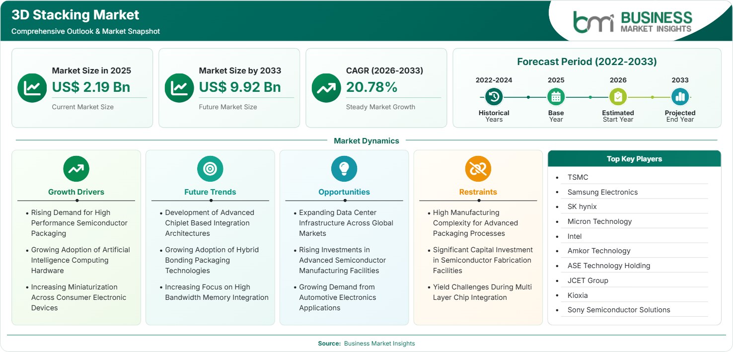
The 3D Stacking Market size was valued at US$ 2.19 billion in 2025 and is projected to reach US$ 9.92 billion by 2033, growing at a CAGR of 20.78% during 2026–2033, driven by advanced semiconductor packaging demand, artificial intelligence hardware expansion, chip miniaturization, high-performance computing requirements, and next-generation electronic device development.

Report Coverage
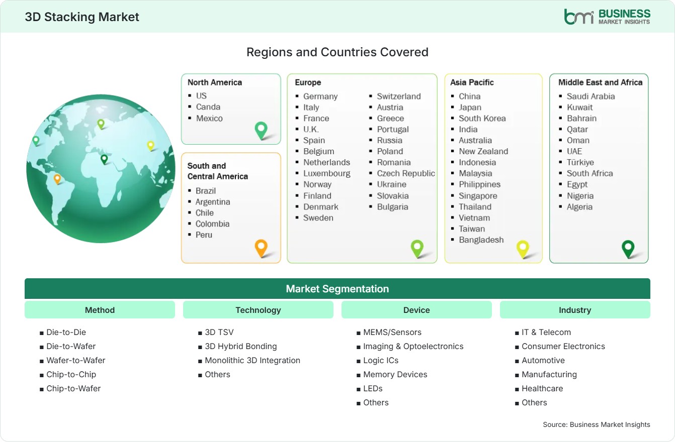
  • Method: Die-to-Die, Die-to-Wafer, Wafer-to-Wafer, Chip-to-Chip, Chip-to-Wafer
  • Technology: 3D TSV , 3D Hybrid Bonding, Monolithic 3D Integration, Others
  • Device: MEMS/Sensors, Imaging & Optoelectronics, Logic ICs, Memory Devices, LEDs, Others
  • Industry: IT & Telecom, Consumer Electronics, Automotive, Manufacturing, Healthcare, Others
US$ 2.19 Bn Market size in 2025
US$ 9.92 Bn Market Size by 2033
20.78% CAGR, 2026 - 2033
2026-2033 Forecast Period

AI Overview

3D Stacking Market Summary

  • North America Region: North America holds a 32%–35% share in 2025 and is projected to grow at a 19.5%–20.5% CAGR during 2026–2033. Growth is supported by semiconductor innovation, artificial intelligence infrastructure, advanced packaging investments, and data center expansion. The U.S. market benefits from strong semiconductor research capabilities, increasing AI hardware demand, and investments in next-generation chip technologies.
  • Fastest Growing Region: Asia Pacific represents a 45%–49% share in 2025 and is expected to expand at a 21.5%–22.5% CAGR during 2026–2033. Growth is driven by semiconductor manufacturing expansion, memory technology advancement, electronics production, and investments by leading chip manufacturers across the region.
  • Leading Segment: Memory Devices account for a 38%–42% share in 2025 and are projected to grow at a 20.2%–21.2% CAGR during 2026–2033. Growth is supported by increasing demand for high-bandwidth memory, artificial intelligence systems, and advanced computing architectures.
  • High Growth Segment: 3D Hybrid Bonding technology represents a 20%–24% share in 2025 and is expected to grow at a 22.0%–23.0% CAGR during 2026–2033. Adoption is supported by improved interconnect density, performance enhancement, and advanced semiconductor packaging requirements.
  • Key Market Opportunity: Expanding artificial intelligence workloads, global data center development, automotive electronics growth, and investments in advanced semiconductor manufacturing are creating opportunities for companies developing high-density stacking solutions.
  • Major Market Players: TSMC, Samsung Electronics Co., Ltd., SK hynix Inc., Micron Technology, Inc., Intel Corporation, Amkor Technology, ASE Technology Holding Co., Ltd., JCET Group, Kioxia Corporation, and Sony Semiconductor Solutions Corporation.
Strategic Insights

3D Stacking Market: Strategic Insights

3D Stacking Market Strategic Framework
FREE PDF
Request your free sample
Request free sample
Stakeholder View

Key Takeaways

  • The market ecosystem includes semiconductor foundries, integrated device manufacturers, packaging companies, equipment providers, and technology developers supporting advanced chip integration.
  • Artificial intelligence computing, high-performance processors, memory-intensive applications, and automotive electronics represent major opportunity areas for companies developing advanced stacking technologies.
  • Innovation is focused on hybrid bonding, through-silicon via advancements, improved thermal management, and enhanced interconnect technologies for next-generation semiconductor architectures.
  • Asia Pacific provides strong investment opportunities due to semiconductor manufacturing concentration, technology leadership, and expanding chip production capabilities.
  • Strategic partnerships among semiconductor manufacturers, foundries, and packaging specialists are increasing to accelerate commercialization of advanced stacking solutions.
  • Companies investing in scalable manufacturing capabilities and advanced packaging expertise are expected to strengthen competitive positioning as semiconductor architectures become more complex.
Geographic Outlook

3D Stacking Market Regional Highlights

North America 3D Stacking Market

North America maintains a significant position due to advanced semiconductor research, artificial intelligence infrastructure development, and strong investments in high-performance computing technologies. The region accounted for 32%–35% share in 2025 and is expected to grow at a 19.5%–20.5% CAGR through 2033. Demand is supported by semiconductor innovation, data center expansion, and increasing adoption of advanced packaging solutions. The region continues strengthening domestic semiconductor capabilities through manufacturing investments and technology development initiatives.

  • Semiconductor companies are increasing investments in advanced packaging technologies to improve chip performance and integration capabilities.
  • Artificial intelligence hardware development is accelerating demand for high-density semiconductor architectures and advanced memory solutions.
  • Data center operators are adopting next-generation processors requiring improved efficiency and computing performance.
  • Research institutions and technology companies are supporting innovation in semiconductor integration techniques.

US 3D Stacking Market

The United States represents the leading North American country market due to strong semiconductor research infrastructure, artificial intelligence development, and increasing investments in domestic chip manufacturing. The country contributes 75%–80% of regional demand and is projected to grow at a 19.8%–20.8% CAGR during 2026–2033. Growth is supported by semiconductor manufacturing initiatives, advanced computing applications, and expanding data center requirements.

  • Semiconductor companies are developing advanced packaging capabilities to support next-generation processors.
  • AI and cloud computing expansion is increasing demand for high-performance semiconductor solutions.
  • Government-supported semiconductor initiatives are encouraging manufacturing investments.
  • Technology companies are increasing collaboration with packaging specialists for advanced chip development.

Europe 3D Stacking Market

Europe demonstrates steady growth due to semiconductor innovation, automotive electronics development, and increasing demand for advanced computing technologies. The region represented a 15%–18% share in 2025 and is expected to grow at a 18.5%–19.5% CAGR through 2033. Germany, France, the Netherlands, and the United Kingdom are important markets supported by automotive semiconductor demand, industrial electronics, and research activities. The region is strengthening semiconductor capabilities through strategic technology investments.

  • Automotive manufacturers are adopting advanced semiconductor architectures for intelligent vehicle systems.
  • Industrial applications are increasing demand for compact and efficient electronic components.
  • Research organizations are supporting semiconductor technology development and packaging innovation.
  • Companies are investing in advanced manufacturing capabilities to improve supply chain resilience.

Asia Pacific 3D Stacking Market

Asia Pacific represents the largest regional market due to semiconductor manufacturing concentration, memory technology leadership, and electronics production capabilities. The region accounted for 45%–49% share in 2025 and is projected to grow at a 21.5%–22.5% CAGR through 2033. China, Taiwan, South Korea, and Japan are major contributors due to strong semiconductor ecosystems and investments in advanced packaging technologies. Growing demand for AI systems and consumer electronics continues supporting regional expansion.

  • Semiconductor manufacturers are expanding advanced packaging facilities to support increasing chip complexity.
  • Memory producers are adopting stacking technologies for high-performance computing applications.
  • Consumer electronics production is increasing demand for compact and efficient semiconductor solutions.
  • Data center expansion is accelerating adoption of advanced memory and processor technologies.
  • Regional governments are supporting semiconductor manufacturing investments and technology development programs.

Rest of World 3D Stacking Market

Latin America, the Middle East, and Africa represent emerging markets supported by digital transformation, electronics adoption, and increasing technology infrastructure development. The region accounts for a 5%–8% share in 2025 and is projected to grow at a 17.5%–18.5% CAGR through 2033. Growing investments in communication infrastructure, industrial automation, and advanced computing applications are creating new opportunities for semiconductor technology providers. Regional adoption remains influenced by technology availability and ecosystem development.

  • Digital infrastructure expansion is increasing demand for advanced electronic systems across emerging economies.
  • Telecommunications development is supporting adoption of high-performance semiconductor components.
  • Industrial automation initiatives are creating opportunities for advanced chip technologies.
  • Technology providers are strengthening regional partnerships to improve market accessibility.
  • Increasing electronics consumption is supporting long-term semiconductor technology adoption.
Global Market Geography
FREE PDF
Request your free sample
Request free sample
Segment Analysis

3D Stacking Market Segmentation

Method

Method segmentation is influenced by integration efficiency, manufacturing compatibility, performance requirements, and application-specific semiconductor architecture needs. Advanced stacking approaches enable higher chip density, improved connectivity, and enhanced processing capabilities. The 3D Stacking Market scope continues expanding as semiconductor manufacturers adopt multiple integration methods to address increasing computational demands.

  • Die-to-Die: Enables direct stacking of individual dies to improve performance and integration flexibility in advanced semiconductor packages.
  • Die-to-Wafer: Supports efficient integration by attaching individual dies onto processed wafers for high-performance applications.
  • Wafer-to-Wafer: Enables large-scale semiconductor integration with improved manufacturing efficiency for advanced devices.
  • Chip-to-Chip: Provides flexible integration of multiple chips for customized electronic architectures.
  • Chip-to-Wafer: Combines chip-level components with wafers to enhance packaging efficiency and performance.

Technology

Technology segmentation reflects advancements in semiconductor integration techniques, interconnect solutions, and packaging architectures. Manufacturers are developing advanced technologies to improve bandwidth, reduce power consumption, and overcome conventional scaling challenges. The 3D Stacking Market trend is shaped by increasing demand for high-performance computing, artificial intelligence processors, and compact electronic designs.

  • 3D TSV (Through Silicon Via): Provides vertical electrical connections between stacked semiconductor layers for improved performance and reduced footprint.
  • 3D Hybrid Bonding: Enables high-density interconnects through direct bonding techniques for advanced memory and logic applications.
  • Monolithic 3D Integration: Integrates semiconductor layers at wafer level to support next-generation chip architectures.
  • Others: Includes emerging stacking technologies supporting specialized semiconductor integration requirements.

Device

Device segmentation highlights increasing adoption of stacked semiconductor architectures across memory, logic, sensing, and optical applications. Different device categories utilize 3D integration to improve processing capability, reduce size, and enhance functionality. The 3D Stacking Market share is influenced by growing requirements for efficient computing, advanced electronics, and high-performance semiconductor devices.

  • MEMS/Sensors: Uses stacked structures to improve sensing performance, compactness, and device functionality.
  • Imaging & Optoelectronics: Supports advanced imaging systems and optical semiconductor applications requiring enhanced integration.
  • Logic ICs: Enables improved processing performance for computing and artificial intelligence applications.
  • Memory Devices: Utilizes stacking technologies to increase storage capacity and bandwidth performance.
  • LEDs: Supports improved device architecture and enhanced performance in lighting applications.
  • Others: Covers additional semiconductor devices adopting advanced stacking solutions.

Industry

Industry segmentation demonstrates broad adoption of 3D stacking technologies across electronics, communication, automotive, healthcare, and industrial sectors. Increasing requirements for compact, efficient, and high-performance electronic systems are driving adoption across multiple industries. The 3D Stacking Market analysis indicates expanding applications as organizations invest in advanced semiconductor capabilities.

  • IT & Telecom: Drives adoption through data centers, networking equipment, and high-performance computing infrastructure.
  • Consumer Electronics: Uses stacked semiconductor solutions for compact and powerful electronic devices.
  • Automotive: Supports advanced vehicle systems, autonomous technologies, and electronic control applications.
  • Manufacturing: Enables automation, industrial computing, and smart production technologies.
  • Healthcare: Supports advanced medical devices and high-performance diagnostic systems.
  • Others: Includes additional industries adopting advanced semiconductor integration technologies.
Market Forces

3D Stacking Market Dynamics

Key Market Drivers

Rising Demand for High Performance Semiconductor Packaging

The increasing complexity of semiconductors and increased computational needs are driving the need for advanced packaging technology. Conventional approaches of scaling technology are facing problems in the area of power effectiveness, heat dissipation, and performance, thereby motivating the manufacturers to implement 3D integration technology. Through 3D stacking, enhanced connectivity, density, and processing performance can be achieved with reduced size. Factors driving the 3D Stacking Market growth include rising demand for the application of artificial intelligence, high-performance computing, and advanced electronics. Semiconductor manufacturers are using advanced packaging technologies in order to enhance the performance of their products. The use of vertical integration technology is becoming crucial for future processors, memories, and computing applications.

Growing Adoption of Artificial Intelligence Computing Hardware

As a result of increased usage of AI-powered technologies, there is an increase in demand for sophisticated semiconductor technology that will be able to cope with complicated operations. AI-powered processors need enhanced memory access, better data handling capabilities, and improved bandwidths, which can be possible through 3D stacked semiconductor architecture. As a result of increased demands on sophisticated computational environments, 3D stacked memory architectures are becoming increasingly popular not only within data centers but also in machine learning systems and specialized AI. Companies manufacturing semiconductors develop advanced semiconductor packages in order to increase performance and control power consumption. Increased spending on AI-related technologies encourages technology firms to apply high-performance semiconductor architectures.

Increasing Miniaturization Across Consumer Electronic Devices

With consumer electronics makers emphasizing compact, lightweight, and functional gadgets, there is an increased need for effective semiconductor integration techniques. Through 3D stacking technology, manufacturers can pack more functions into a small space while improving the functionality of devices. Increasingly, smartphones, wearable devices, and other portable gadgets need advanced chip structures that offer computing functionalities. The 3D Stacking Market trend is indicative of increased use of vertically-integrated semiconductor techniques to overcome challenges associated with size and performance issues. With increased demand from consumers for improved electronic gadgets, manufacturers have been developing advanced packaging solutions. Through multi-layered semiconductors, manufacturers are able to increase the efficiency and functionalities of gadgets without changing their sizes.

Key Market Opportunities

Expanding Data Center Infrastructure Across Global Markets

The increasing need for cloud computing, artificial intelligence solutions, and digital infrastructure is giving rise to many opportunities regarding 3D stacking technology usage. The need for advanced semiconductor solutions that offer increased processing capabilities, energy efficiency, and memory bandwidth is growing in data centers. Advanced memory stacking and packaging technology becomes an integral part of high-performance computing systems. Companies operating in the semiconductor industry could take advantage of solutions focused on solving problems arising in data-intensive applications. An increasing number of cloud infrastructure installations in emerging markets is driving growth in the need for advanced computing components.

Rising Investments in Advanced Semiconductor Manufacturing Facilities

Rising investment in fabs and packaging plants has created opportunities for firms engaged in advanced stacking technology. Governments and tech firms are enhancing the semiconductor ecosystem to increase manufacturing capability and robustness of their supply chains. The 3D Stacking Market forecast shows a growing opportunity as manufacturers expand production capacity for advanced semiconductors and advanced packaging technology. Fabrication plants are implementing advanced integration technologies that will be used in future semiconductors. Firms investing in the development of equipment, materials, and manufacturing know-how will benefit from rising investment. The increasing complexity of semiconductors is driving collaboration among foundries, packaging firms, and technology firms.

Growing Demand from Automotive Electronics Applications

Automotive electronics are opening up many new possibilities for the application of 3D stacking as automobiles become sophisticated in computing and connectivity. Electric cars, self-driving capabilities, and advanced driver assistance systems require efficient, compact semiconductors with enhanced performance. 3D stacking allows automakers to pack in more functionality and performance despite space constraints. Automakers are partnering with semiconductor suppliers to design sophisticated electronic architectures. The rise in electric vehicles and digitalization is driving demand for innovation in semiconductor chips. Semiconductor manufacturers that cater to automobile applications can benefit from a range of application opportunities.

Market Restraints and Challenges

High Manufacturing Complexity for Advanced Packaging Processes

Factor: 3D stacking requires high manufacturing precision, high-end equipment, specialized materials, and advanced integration procedures. Impact: Manufacturing difficulties may lead to production issues, lower yields, and complications in commercial implementation. The semiconductor companies are making efforts to improve their manufacturing processes, automate operations, and implement advanced quality control systems to overcome these problems. The development of manufacturing processes is very important for increasing efficiency and minimizing production risks. The difficulties associated with multiple layers of integration continue to affect development timelines and production costs. Advanced technology and scalable procedures are important for overcoming these difficulties.

Significant Capital Investment in Semiconductor Fabrication Facilities

Factor: Highly sophisticated manufacturing and packing facilities for semiconductors involve significant amounts of capital investment in terms of machines, R&D, infrastructure, and manufacturing systems. Impact: Significant capital investments often impose constraints on small businesses and create financial strain during the development process. To overcome such issues, semiconductor companies have taken a number of initiatives, including strategic partnerships, joint investments, and capacity planning. An increase in production capability requires effective resource and technology management. Companies are prioritizing scalable options to ensure higher returns on investment in the future.

Company Analysis

Competitive Landscape

The 3D Stacking Market analysis highlights competition among semiconductor manufacturers, foundries, packaging specialists, and technology providers developing advanced vertical integration solutions. Leading companies are focusing on hybrid bonding, advanced packaging capabilities, high-performance memory technologies, and strategic collaborations to strengthen their positions across artificial intelligence, data centers, consumer electronics, automotive, and industrial applications.

Company Name

Overview

Products and Services relevant to this market

TSMC

Leading semiconductor foundry providing advanced manufacturing and packaging technologies globally.

Offers advanced 3D IC packaging solutions, wafer technologies, and semiconductor integration services.

Samsung Electronics Co., Ltd.

Global technology company involved in semiconductor manufacturing, memory, and advanced chip solutions.

Provides 3D stacked memory solutions, advanced packaging technologies, and semiconductor manufacturing capabilities.

SK hynix Inc.

Semiconductor company specializing in memory technologies and high-performance computing solutions.

Develops stacked memory products including advanced high-bandwidth memory solutions for computing applications.

Micron Technology, Inc.

Semiconductor manufacturer focused on memory and storage technologies.

Provides advanced memory products and stacked semiconductor solutions for computing and electronic applications.

Intel Corporation

Technology company developing processors, semiconductor technologies, and advanced packaging platforms.

Offers advanced packaging solutions, 3D integration technologies, and processor architectures.

Amkor Technology

Semiconductor packaging and testing company serving global technology markets.

Provides advanced packaging, wafer-level solutions, and 3D semiconductor integration services.

ASE Technology Holding Co., Ltd.

Semiconductor assembly and testing provider supporting advanced packaging requirements.

Offers packaging technologies, chip integration solutions, and semiconductor manufacturing services.

JCET Group

Semiconductor packaging and testing company with global manufacturing capabilities.

Provides advanced packaging, wafer-level packaging, and integrated semiconductor solutions.

Kioxia Corporation

Semiconductor company specializing in memory technologies and storage solutions.

Develops flash memory technologies and stacked memory architectures for advanced applications.

Sony Semiconductor Solutions Corporation

Semiconductor business focused on imaging, sensing, and electronic components.

Provides stacked image sensors, semiconductor devices, and advanced integration technologies.

Trust & Transparency

Research Methodology

The market analysis combines proprietary research with secondary data from government agencies, company disclosures, regulatory filings, industry databases and expert interviews. Market estimates are validated through data triangulation, cross-market benchmarking and analyst review.

View Full Research Methodology

Questions Answered

Frequently Asked Questions

What does the 3D Stacking Market report indicate about future competition?

The report indicates that competition will focus on advanced packaging innovation, hybrid bonding capabilities, manufacturing scalability, and high-performance semiconductor solutions. Companies developing efficient integration technologies and strengthening semiconductor partnerships are expected to improve their competitive positioning.

Why are artificial intelligence applications creating new opportunities for 3D stacking solutions?

Artificial intelligence applications require powerful processors, high-bandwidth memory, and efficient data processing capabilities. 3D stacking supports these requirements by enabling closer integration between computing and memory components, improving performance for demanding AI workloads.

How are advanced semiconductor technologies influencing 3D stacking adoption?

Advanced semiconductor technologies are increasing adoption by enabling improved hybrid bonding, through-silicon via integration, thermal management, and multi-layer chip architectures. Manufacturers are using these innovations to overcome conventional scaling limitations and develop higher-performance semiconductor solutions.

Which applications present the strongest opportunity in the market?

Artificial intelligence computing, data centers, memory devices, automotive electronics, and advanced consumer electronics represent strong opportunities. These applications require higher processing capability, improved bandwidth, and compact semiconductor architectures that support increasing technology requirements.

What factors are improving 3D Stacking Market return on investment?

Increasing demand for high-performance computing, artificial intelligence hardware, advanced memory solutions, and compact semiconductor designs is improving return on investment. 3D stacking enables higher integration density, improved performance, and enhanced energy efficiency, making it valuable for next-generation electronic applications.

Access the Full 3D Stacking Market Report

Get segment-level forecasts, regional estimates, competitive benchmarking, company profiles and downloadable Excel datasets.

Access the full 3D Stacking Market Report
350 pages PDF & Excel | 2026-08-25
Similar Research

Related Market Reports