
Semiconductor Bonding Market Outlook: Size, Share, Trends, Growth Analysis, Competitive Landscape & Forecast, 2026-2033

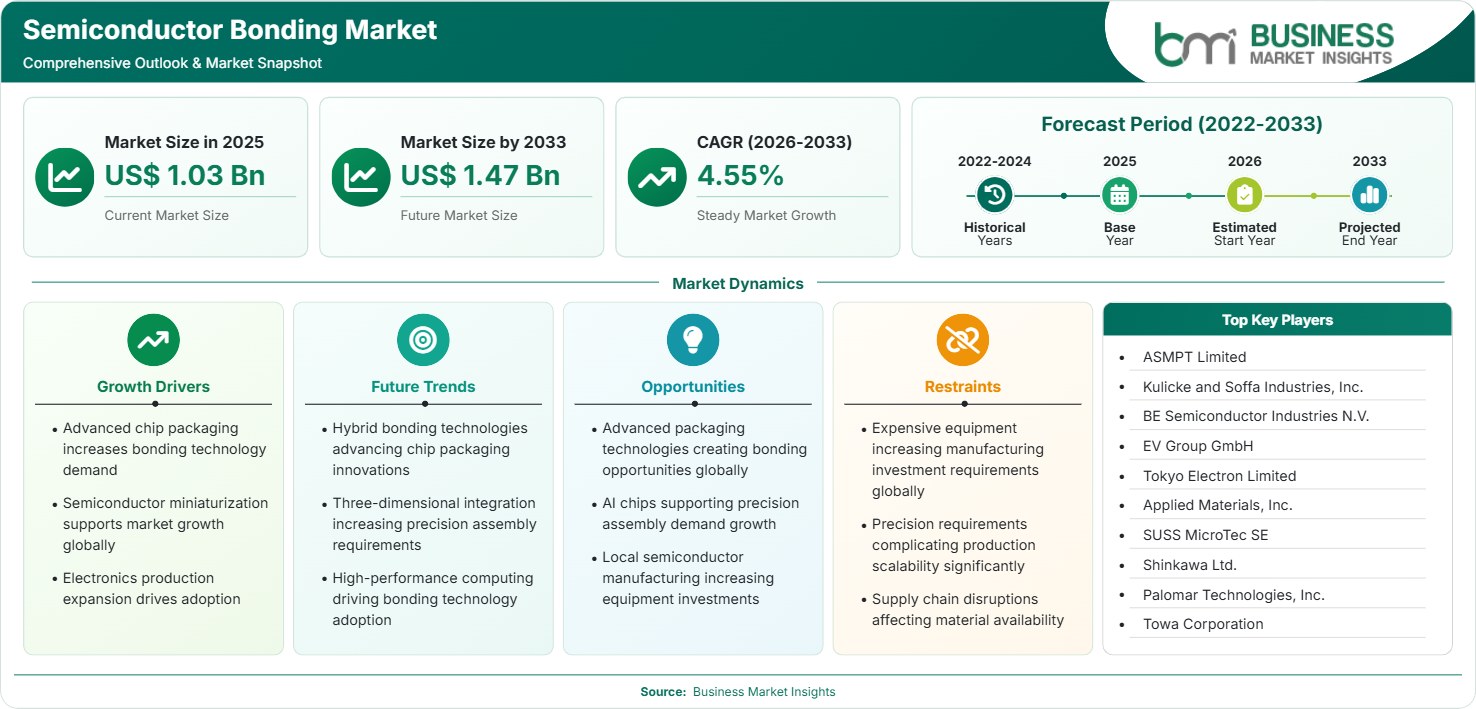
The Semiconductor Bonding Market size was valued at US$ 1.03 Billion in 2025 and is projected to reach US$ 1.47 Billion by 2033, growing at a CAGR of 4.55% during 2026–2033. Growth is supported by advanced packaging adoption, rising AI processor demand, 3D semiconductor integration, heterogeneous chip architectures, expanding wafer-level manufacturing, and increasing investments in high-performance computing and automotive electronics.

Report Coverage
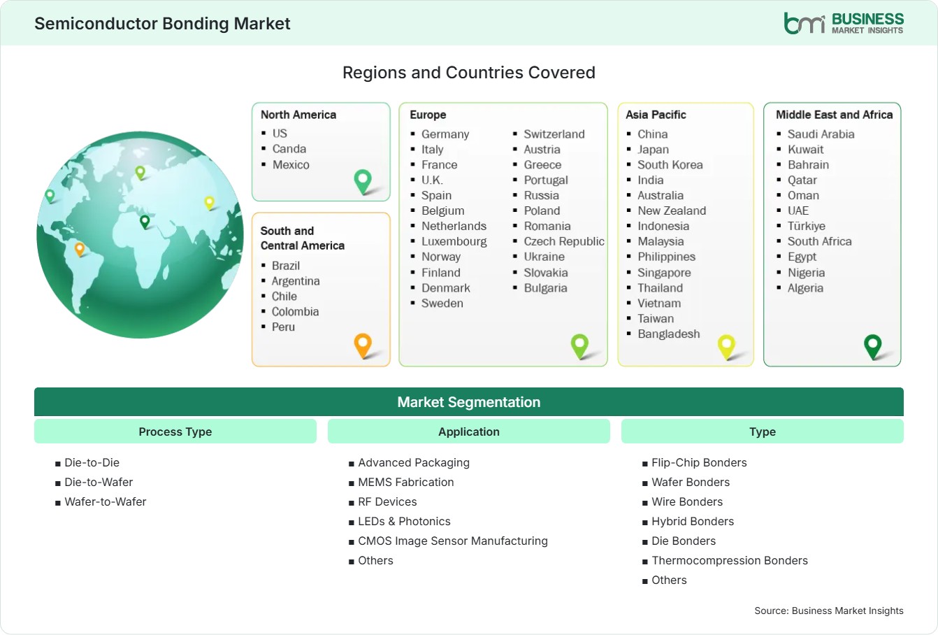
  • Process Type: Die-to-Die, Die-to-Wafer, Wafer-to-Wafer
  • Application: Advanced Packaging, MEMS Fabrication, RF Devices, LEDs & Photonics, CMOS Image Sensor Manufacturing, Others
  • Type: Flip-Chip Bonders, Wafer Bonders, Wire Bonders, Hybrid Bonders, Die Bonders, Thermocompression Bonders, Others
US$ 1.03 Bn Market size in 2025
US$ 1.47 Bn Market Size by 2033
4.55% CAGR, 2026 - 2033
2026-2033 Forecast Period

AI Overview

Semiconductor Bonding Market Summary

  • North America Region: North America holds a 22%–25% share in 2025, expanding at a 4.0%–4.4% CAGR during 2026–2033. Growth is supported by advanced packaging investments, AI semiconductor demand, domestic manufacturing initiatives, defense electronics requirements, supply chain localization efforts, chiplet architecture adoption, and expanding research partnerships across major fabrication ecosystems. Brief US market analysis: The US represents 72%–76% of North American demand and advances at 4.2%–4.6% CAGR, driven by CHIPS Act investments and packaging innovation.
  • Fastest Growing Region: Asia Pacific accounts for 42%–45% share in 2025, registering a 5.2%–5.8% CAGR through 2033. Growth stems from semiconductor fabrication expansion, memory manufacturing dominance, advanced packaging leadership, government incentives, increasing electronics exports, AI infrastructure deployment, and rising capital expenditure across foundries and OSAT facilities.
  • Leading Segment: Wire Bonders command a 28%–31% share in 2025 and grow at 3.8%–4.2% CAGR. Continued adoption in power semiconductors, automotive electronics, industrial modules, mature-node manufacturing, cost-sensitive packaging operations, reliability-focused assembly, and large installed production bases sustains segment leadership worldwide.
  • High Growth Segment: Hybrid Bonders represent 10%–13% Semiconductor Bonding Market share in 2025 and expand at 8.0%–8.8% CAGR. Demand is driven by chiplet architectures, high-bandwidth memory integration, heterogeneous packaging, AI accelerators, advanced logic devices, fine-pitch interconnect requirements, and next-generation three-dimensional semiconductor stacking technologies.
  • Key Market Opportunity: Rapid commercialization of hybrid bonding for AI processors, memory stacks, and heterogeneous integration creates opportunities for equipment suppliers, precision materials providers, foundries, packaging specialists, and semiconductor manufacturing ecosystems globally.
  • Major Market Players: ASMPT Limited, Kulicke and Soffa Industries, Inc., BE Semiconductor Industries N.V., EV Group GmbH, Tokyo Electron Limited, Applied Materials, Inc., SUSS MicroTec SE, Shinkawa Ltd., Palomar Technologies, Inc., and Towa Corporation.
Strategic Insights

Semiconductor Bonding Market: Strategic Insights

Semiconductor Bonding Market Strategic Framework
FREE PDF
Request your free sample
Request free sample
Stakeholder View

Key Takeaways

  • The value chain is becoming more integrated since equipment vendors are working closely with foundries, OSAT providers, substrate suppliers, and advanced packaging specialists to improve interconnect density and manufacturing yields.
  • The strongest long-term potential is found in hybrid bonding and advanced packaging applications since AI accelerators, high-performance computing processors, and heterogeneous integration platforms all require ever more sophisticated assembly technologies.
  • Innovation is now aiming at achieving sub-micron alignment accuracy, using copper-to-copper hybrid bonding, incorporating automated inspection, and developing high-throughput production systems that can support future chiplet architectures.
  • The investment case in Asia Pacific is the most attractive because of its extensive fabrication capacity, the growing advanced packaging infrastructure, and government-supported semiconductor industrial policies.
  • As suppliers aim to obtain different capabilities in wafer-level and die-level integration technologies, there has been an increase in strategic acquisitions, research partnerships, and packaging ecosystem alliances.
  • The demand for reliable bonding solutions, which are needed to support power devices, sensors, and long-life semiconductor modules, is increasing due to the growth of automotive electrification and industrial automation.
Geographic Outlook

Semiconductor Bonding Market Regional Highlights

North America Semiconductor Bonding Market

North America accounted for 22%–25% of global revenue in 2025 and is projected to grow at 4.0%–4.4% CAGR through 2033. The Semiconductor Bonding Market share remains supported by established research ecosystems and strategic domestic supply-chain initiatives. Major equipment procurement continues among packaging facilities pursuing higher interconnect density, improved performance, and advanced heterogeneous integration capabilities.

  • Investments supported by the CHIPS Act are helping to enhance domestic packaging capabilities and are at the same time promoting the upgrading of equipment in both assembly and packaging operations.
  • The production of AI accelerators is leading to a greater demand for high-precision bonding systems that are capable of supporting the integration of advanced memory and processors.
  • Because highly reliable assembly technologies are needed for defense and aerospace electronics programs, there is a continuous demand for top-quality equipment.
  • The exchange of research among universities, foundries, and equipment suppliers speeds up process innovation and its commercialization.

US Semiconductor Bonding Market

The United States represents 72%–76% of North American Semiconductor Bonding Market demand and is expected to expand at 4.2%–4.6% CAGR. Strong activity in advanced packaging, AI processors, defense electronics, and domestic semiconductor manufacturing supports equipment adoption.

  • The demand for hybrid and wafer bonding solutions is growing due to increased investments in advanced packaging facilities.
  • The greater the extent to which AI infrastructure is deployed, the more there will be a need for packaging technologies that support the integration of high-bandwidth memory.
  • The expansion of semiconductor manufacturing, which is backed by the government, leads to increased equipment procurement.
  • Research leadership facilitates the early adoption of new interconnect and chiplet assembly methods.

Europe Semiconductor Bonding Market

Europe holds 19%–22% Semiconductor Bonding Market share in 2025 and is forecast to achieve 4.1%–4.7% CAGR during 2026–2033. Germany remains the leading market, while Ireland and Italy demonstrate stronger growth trajectories. Regional demand is supported by automotive semiconductors, industrial electronics, MEMS manufacturing, and strategic semiconductor sovereignty initiatives.

  • Germany's demand is highest because of its production of automotive semiconductors and its leadership in industrial automation.
  • Ireland gains the benefits of semiconductor investment schemes and the expansion of manufacturing by multinational companies.
  • The production of MEMS and sensors is supporting the stable adoption of wafer bonding technologies.
  • The initiatives under the European Chips Act are aimed at modernizing infrastructure and enhancing supply-chain resilience.
  • Research institutes have a significant role in speeding up innovation in advanced packaging.

Asia Pacific Semiconductor Bonding Market

Asia Pacific accounts for a 42%–45% share in 2025 and records the highest growth at 5.2%–5.8% CAGR. The region dominates global packaging and assembly activities, supporting strong Semiconductor Bonding Market growth. Extensive foundry capacity and government incentives continue driving equipment deployment and process upgrades.

  • Taiwan retains its leadership due to its advanced foundry and packaging infrastructure.
  • South Korea has the advantage of producing memory semiconductors, which require advanced interconnect technologies.
  • China is still making heavy investments in achieving self-sufficiency in semiconductors and in expanding its manufacturing capacity.
  • India is becoming a destination for packaging and assembly, due to policy incentives.
  • The demand from both AI and high-performance computing is pushing towards the wider adoption of hybrid bonding solutions.

Rest of World Semiconductor Bonding Market

Rest of World contributes 11%–14% Semiconductor Bonding Market share in 2025 and is anticipated to register 4.5%–5.0% CAGR through 2033. In South and Central America, Brazil leads semiconductor assembly activity. Within the Middle East and Africa, the United Arab Emirates and Saudi Arabia are advancing electronics manufacturing capabilities.

  • Brazil is still the main focus for the assembly of electronics and for manufacturing activities related to semiconductors.
  • The United Arab Emirates is enhancing its investments in technology infrastructure and in advanced manufacturing capabilities.
  • Saudi Arabia is supporting the development of its electronics ecosystem as part of its industrial diversification efforts.
  • The formation of multinational partnerships is helping to improve access to semiconductor manufacturing expertise in the region.
  • The increasing demand for consumer and industrial electronics is helping to drive long-term growth in the market.
Global Market Geography
FREE PDF
Request your free sample
Request free sample
Segment Analysis

Semiconductor Bonding Market Segmentation

Process Type

Process Type represented approximately 33%–36% market share in 2025 and is expected to expand at 4.8%–5.2% CAGR. Growing demand for advanced packaging, chiplet integration, and high-density interconnect architectures is broadening adoption across semiconductor manufacturing. The Semiconductor Bonding Market scope continues to expand as producers pursue higher performance and greater miniaturization through wafer-level and die-level integration approaches.

  • Die-to-Die: Supports heterogeneous integration requirements by enabling assembly of optimized chip components, improving performance, flexibility, and design scalability in advanced computing applications.
  • Die-to-Wafer: Gains momentum from chiplet architectures requiring efficient placement accuracy, high throughput, and cost-effective production workflows.
  • Wafer-to-Wafer: Widely utilized in high-volume manufacturing applications where alignment precision, productivity, and process consistency remain critical.

Application

Application-related demand accounts for approximately 38%–41% of the Semiconductor Bonding Market share in 2025 and advances at a 4.9%–5.4% CAGR. Expanding deployment across AI computing, sensing technologies, automotive electronics, and optical communication solutions drives equipment demand. Increasing performance requirements encourage broader utilization of both traditional and advanced bonding methodologies.

  • Advanced Packaging: Enables higher interconnect density, improved power efficiency, and enhanced device functionality needed for emerging semiconductor architectures.
  • Micro-Electro-Mechanical Systems (MEMS) Fabrication: Relies on wafer bonding technologies for sensors, actuators, and micro-scale device manufacturing applications.
  • RF Devices: Demand precise assembly methods supporting signal integrity, miniaturization, and performance across wireless communication systems.
  • LEDs & Photonics: Bonding technologies facilitate optical integration and packaging improvements required for high-performance photonic applications.
  • CMOS Image Sensor (CIS) Manufacturing: Benefits from advanced wafer stacking approaches that enhance imaging capability and device efficiency.

Type

Type-based demand represents around 44%–47% market share in 2025 and is expected to expand at 4.6%–5.0% CAGR. The market reflects a combination of mature wire-bonding solutions and emerging hybrid-bonding platforms. Semiconductor Bonding Market trends increasingly favor technologies supporting advanced packaging and heterogeneous integration requirements.

  • Flip-Chip Bonders: Enable direct chip-to-substrate attachment, providing superior electrical performance and package density.
  • Wafer Bonders: Essential for MEMS, sensors, and advanced packaging applications requiring precise wafer-level integration.
  • Wire Bonders: Maintain extensive deployment because of established manufacturing infrastructure, reliability, and cost-effectiveness.
  • Hybrid Bonders: Support ultra-fine interconnect pitches and next-generation three-dimensional semiconductor architectures.
  • Die Bonders: Serve diverse assembly requirements across consumer, industrial, and automotive semiconductor production.
  • Thermocompression Bonders: Offer robust interconnection performance required for demanding packaging applications.
Market Forces

Semiconductor Bonding Market Dynamics

Key Market Drivers

Increasing Complexity of Advanced Semiconductor Packaging

Advanced processors and heterogeneous systems combine multiple dies to improve functionality without relying exclusively on monolithic scaling. These architectures increase requirements for alignment accuracy, interconnect density, and process repeatability. The supplied global forecast implies expansion from US$ 1.03 billion in 2025 to US$ 1.47 billion in 2033, at a 4.55% CAGR during 2026–2033. The Semiconductor Bonding Market growth opportunity is therefore tied to production-qualified integration technologies rather than device miniaturization alone.

Demand for High-Bandwidth Memory and Chiplet Integration

With higher-performance computing, there is greater demand for efficient connections among processors, memory stacks, and specialized accelerators. Although chiplet architectures enable manufacturers to combine components that have been made using different process technologies, they also call for more stringent assembly requirements. The bonding equipment must ensure accurate placement, achieve controlled contact formation, and be compatible with ever denser structures. Methods such as thermocompression and hybrid bonding deal with the various requirements that arise during this transition.

Expansion of Sensor and Specialized Semiconductor Manufacturing

MEMS, CMOS image sensors, RF components, and photonic devices require bonding processes tailored to their physical and electrical characteristics. MEMS devices may require cavity sealing or controlled-atmosphere packaging, while imaging and photonic products demand precise alignment and contamination management. These requirements broaden equipment demand beyond advanced logic packaging. Equipment vendors can serve multiple applications by offering configurable platforms, process modules, and application engineering. The Semiconductor Bonding Market trends also reflect the need to transfer processes from development lines into repeatable manufacturing.

Key Market Opportunities

Commercialization of Hybrid Bonding for High-Density Integration

Hybrid bonding offers opportunities where conventional interconnect approaches struggle to meet density and performance requirements. Its adoption can create demand for bonding platforms, surface preparation tools, alignment systems, and advanced metrology. Commercialization nevertheless requires validated process windows, low defect rates, and acceptable manufacturing economics. Equipment suppliers can invest in joint development programs with logic, memory, and packaging manufacturers to accelerate qualification. Semiconductor Bonding Market Forecasts should therefore distinguish early-stage development interest from confirmed commercial installations and repeat equipment orders.

Integration of Bonding Equipment with Automated Metrology

The use of automated inspection and alignment measurements offers a chance to improve yield control and decrease the need for manual work. By integrating bonding systems with metrology, manufacturers will be able to detect placement errors, surface defects, and process drift at an earlier stage in the production process. Suppliers could create combined packages of equipment, software, and services that cover the entire process sequence rather than just one bonding step. The case for making an investment becomes stronger when production volumes are large, and the losses resulting from defects are costly. Collaborations between equipment producers and metrology experts can lead to more consistent data collection, process correction, and qualification.

Expansion into MEMS, Photonics, and Specialized Packaging

Equipment suppliers can continue manufacturing specialized devices by adjusting their bonding systems to accommodate different materials, wafer sizes, and sealing requirements. In the case of MEMS production, hermetic packaging is required, whereas photonic integration relies on precise optical alignment and controlled interfaces. RF and imaging applications also call for specific process requirements that cannot be met by general-purpose assembly tools. It is therefore possible for vendors to make investments in application-specific modules, process development, and regional technical support.

Market Restraints and Challenges

High Equipment Costs and Lengthy Qualification Cycles

The use of advanced bonding systems entails a large initial outlay, requires specialized facilities, demands significant process development resources, and requires integration with inspection and handling equipment. As a result, smaller manufacturers might put their purchases off, continue to use traditional bonding methods, or restrict the use of advanced systems to pilot lines until the production economics are better understood. Moreover, the qualification process can lengthen the time taken to make procurement decisions since device manufacturers have to demonstrate reliability and yield under various operating conditions.

Process Sensitivity and Manufacturing Yield Risks

The bonding performance is influenced by the cleanliness of the surface, the flatness of the wafer, the compatibility of the materials, the thermal conditions, the pressure distribution, and the accuracy of alignment. This means that minor variations can lead to defects, lower yield, and higher rework costs, especially in advanced packaging structures which have a large number of interconnected components. Processes involving hybrids and wafer-level techniques may need more rigorous process control than those used in traditional assembly methods.

Company Analysis

Competitive Landscape

The competitive environment remains shaped by advanced packaging innovation, precision engineering expertise, and customer-specific process development. Current Semiconductor Bonding Market analysis indicates leadership among established bonding-equipment providers serving global foundries, OSAT companies, memory manufacturers, and semiconductor integrated device producers.

Company Name

Overview

Products and Services relevant to this market

ASMPT Limited

Global semiconductor assembly equipment supplier with strong advanced packaging and automation capabilities.

Die bonders, wire bonders, packaging systems, process optimization solutions.

Kulicke and Soffa Industries, Inc.

Major provider of semiconductor interconnect and assembly equipment worldwide.

Wire bonders, advanced packaging equipment, services, software solutions.

BE Semiconductor Industries N.V.

Leading advanced packaging equipment manufacturer serving high-end semiconductor applications.

Hybrid bonding systems, die attach equipment, flip-chip bonding solutions.

EV Group GmbH

Specialist in wafer bonding and lithography technologies for advanced manufacturing.

Wafer bonders, hybrid bonding tools, alignment and metrology platforms.

Tokyo Electron Limited

Global semiconductor equipment company with broad fabrication and packaging portfolio.

Bonding solutions, wafer processing systems, advanced packaging equipment.

Applied Materials, Inc.

Major semiconductor equipment supplier focused on process innovation.

Hybrid bonding platforms, packaging systems, semiconductor manufacturing technologies.

SUSS MicroTec SE

Precision equipment provider supporting wafer-level manufacturing processes.

Wafer bonders, lithography systems, process development solutions.

Shinkawa Ltd.

Established semiconductor assembly specialist with global market presence.

Wire bonding systems, advanced packaging equipment, manufacturing solutions.

Palomar Technologies, Inc.

Precision microelectronics assembly provider serving specialized applications.

Die bonders, micro-assembly systems, packaging technologies.

Towa Corporation

Semiconductor packaging equipment manufacturer with extensive global footprint.

Packaging, molding, assembly, and bonding-related equipment solutions.

Trust & Transparency

Research Methodology

The market analysis combines proprietary research with secondary data from government agencies, company disclosures, regulatory filings, industry databases and expert interviews. Market estimates are validated through data triangulation, cross-market benchmarking and analyst review.

View Full Research Methodology

Questions Answered

Frequently Asked Questions

What does a Semiconductor Bonding Market Report typically evaluate?

A Semiconductor Bonding Market Report generally examines market size, technology trends, competitive positioning, regional developments, segment performance, investment patterns, and future growth opportunities across end-use applications.

What factors influence equipment purchasing decisions?

Manufacturers primarily evaluate alignment precision, throughput, yield improvement potential, reliability, automation features, total ownership costs, and compatibility with existing production infrastructure.

Why is Asia Pacific leading industry demand?

The region hosts significant foundry, memory, packaging, and assembly capacity, supported by industrial policies, mature supply chains, and ongoing semiconductor manufacturing investments.

What application area creates the strongest future demand?

AI accelerators, high-performance computing processors, and high-bandwidth memory packages are expected to generate substantial demand because they require advanced packaging and high-density interconnect solutions.

How does bonding technology support advanced semiconductor packaging?

Bonding technologies enable integration of multiple chips, sensors, and memory components into compact architectures that improve performance, power efficiency, and functionality while supporting miniaturization requirements.

Access the Full Semiconductor Bonding Market Report

Get segment-level forecasts, regional estimates, competitive benchmarking, company profiles and downloadable Excel datasets.

Access the full Semiconductor Bonding Market Report
350 pages PDF & Excel | 2026-10-28
Similar Research

Related Market Reports