
Semiconductor Plating System Market Outlook: Size, Share, Trends, Growth Analysis, Competitive Landscape & Forecast, 2026-2033

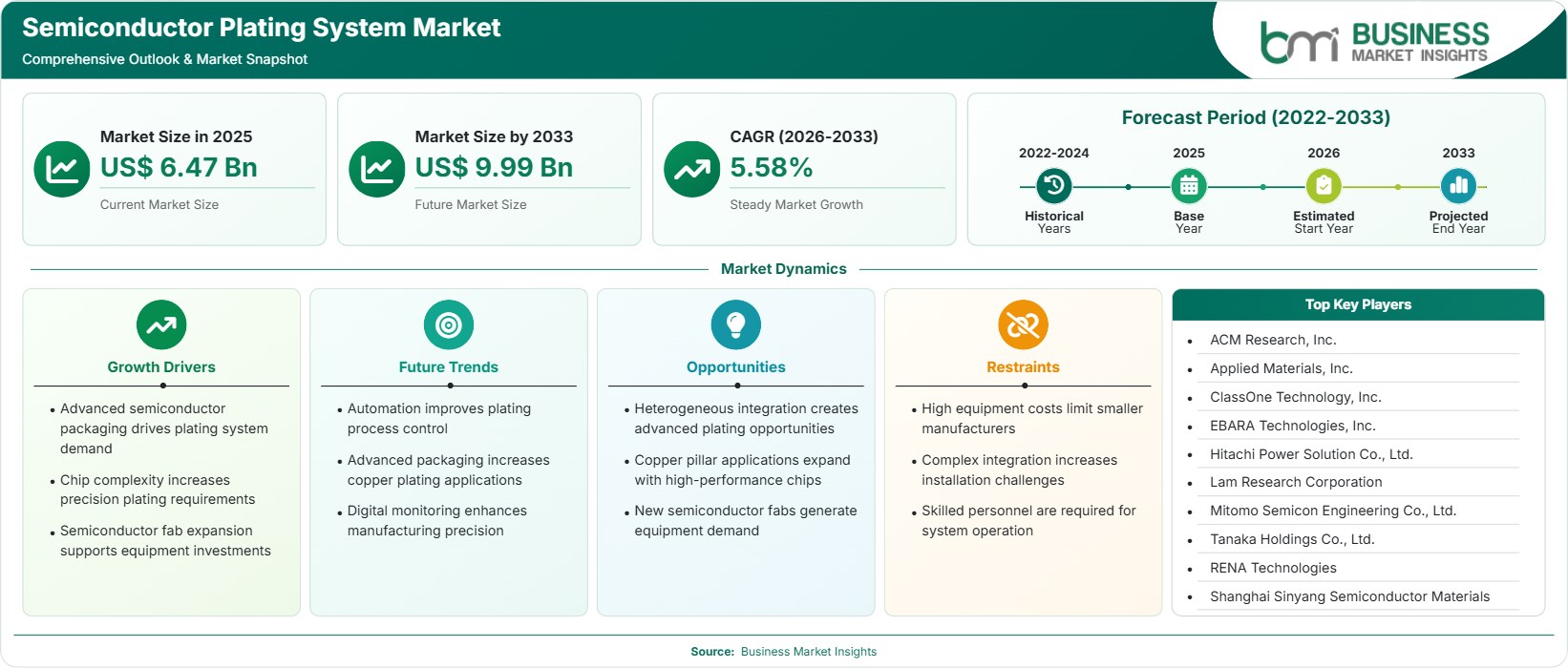
The Semiconductor Plating System Market size was valued at USD 6.47 Billion in 2025 and is projected to reach USD 9.99 Billion by 2033, growing at a CAGR of 5.58% during 2026–2033. Growing semiconductor packaging complexity, expanding advanced-node production, increasing investment in wafer-level packaging, and rising demand for AI, automotive, and high-performance computing chips continue creating substantial market opportunities.

Report Coverage
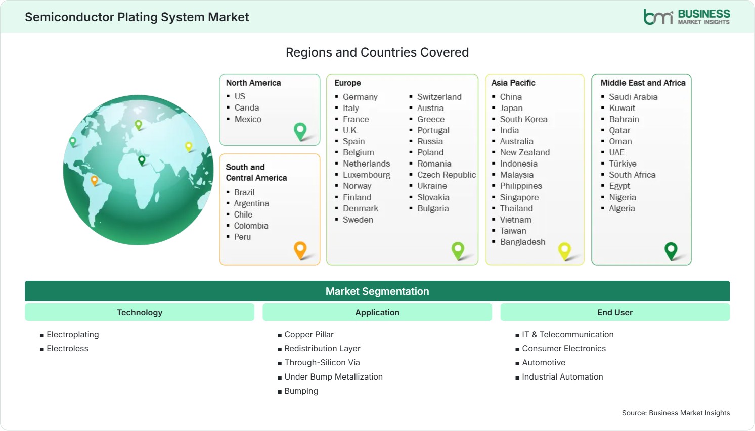
  • Technology: Electroplating, Electroless
  • Application: Copper Pillar, Redistribution Layer, Through-Silicon Via, Under Bump Metallization, Bumping
  • End User: IT & Telecommunication, Consumer Electronics, Automotive, Industrial Automation
US$ 6.47 Bn Market size in 2025
US$ 9.99 Bn Market Size by 2033
5.58% CAGR, 2026 - 2033
2026-2033 Forecast Period

01 AI Overview

Semiconductor Plating System Market Summary

  • North America Region: North America holds 21%–24% share in 2025 and is projected to grow at a 5.2%–5.8% CAGR during 2026–2033. Strong semiconductor manufacturing investments, expanding advanced packaging capacity, growing CHIPS-related funding initiatives, and increasing demand for high-performance computing devices continue driving equipment adoption. U.S. market expansion is supported by fab investments and advanced packaging projects, growing at 5.3%–5.9% CAGR.
  • Fastest Growing Region: Asia Pacific accounts for 47%–51% share in 2025 and is forecast to expand at a 6.2%–6.9% CAGR during 2026–2033. Expanding semiconductor fabrication capacity, advanced packaging investments, rising electronics production, and strong government support continue accelerating equipment procurement.
  • Leading Segment: Electroplating represents 69%–73% share in 2025 and is expected to grow at a 5.6%–6.2% CAGR. Broad adoption in wafer-level packaging, redistribution layers, copper interconnects, and advanced packaging processes supports segment leadership.
  • High Growth Segment: Through-Silicon Via (TSV) accounts for 17%–21% share in 2025 and is projected to expand at a 6.8%–7.5% CAGR. Rising adoption of 3D packaging architectures, AI processors, and high-bandwidth memory solutions continues accelerating deployment.
  • Key Market Opportunity: Expansion of heterogeneous integration, advanced packaging technologies, and next-generation semiconductor architectures creates opportunities for precision plating systems that support higher performance, miniaturization, and manufacturing efficiency.
  • Major Market Players: ACM Research, Inc., Applied Materials, Inc., ClassOne Technology, Inc., EBARA Technologies, Incorporated, Hitachi Power Solutions Co., Ltd., Lam Research Corporation, Mitomo Semicon Engineering Co., Ltd., TANAKA Holdings Co., Ltd., RENA Technologies GmbH, Shanghai Sinyang Semiconductor Materials Co., Ltd.
02 Strategic Insights

Semiconductor Plating System Market: Strategic Insights

Semiconductor Plating System Market Strategic Framework
FREE PDF
Request your free sample
Request free sample
03 Stakeholder View

Key Takeaways

  • The supply chain increasingly integrates plating-equipment suppliers, semiconductor foundries, OSAT providers, material manufacturers, and automation specialists to optimize advanced packaging processes.
  • TSV, redistribution layer, and copper pillar applications present the strongest growth opportunities due to increasing adoption of advanced packaging architectures.
  • Innovation efforts are increasingly focused on process uniformity, automation, AI-driven process control, and high-throughput plating platforms.
  • Asia Pacific remains the most attractive regional investment destination because of its concentration of semiconductor fabrication and packaging capacity.
  • Strategic investments in advanced packaging facilities and semiconductor supply-chain localization continue stimulating equipment demand.
  • Demand from AI accelerators, data-center processors, and automotive semiconductors is reshaping capital expenditure priorities throughout the semiconductor ecosystem.
04 Geographic Outlook

Semiconductor Plating System Market Regional Highlights

North America Semiconductor Plating System Market

North America represented 21%–24% Semiconductor Plating System Market share in 2025 and is projected to expand at a 5.2%–5.8% CAGR through 2033. Strong government support, semiconductor reshoring initiatives, and expansion of advanced packaging capabilities continue supporting regional demand. Leading semiconductor manufacturers are investing in high-performance packaging technologies to address growing demand from artificial intelligence, automotive, and cloud-computing applications. The combination of technology innovation and domestic manufacturing initiatives continues strengthening market activity.

  • Large-scale fabrication and advanced packaging investments are driving procurement of precision plating equipment for next-generation semiconductor production.
  • Semiconductor reshoring programs continue supporting adoption of advanced manufacturing technologies and capital equipment upgrades.
  • Increasing demand for AI processors and data-center semiconductors is accelerating advanced packaging requirements.
  • Automation and process-control improvements remain major investment priorities among semiconductor manufacturers.
  • Strong collaboration between equipment suppliers and semiconductor producers supports rapid technology deployment.

US Semiconductor Plating System Market

The United States accounts for approximately 81%–85% share within North America and is expected to grow at a 5.3%–5.9% CAGR during 2026–2033. Expansion of fabrication facilities, increasing investments in advanced packaging technologies, and rising semiconductor demand across strategic industries support national market leadership. Equipment suppliers continue benefiting from significant investment activity associated with chip manufacturing modernization and supply-chain resilience initiatives.

  • Advanced packaging facilities continue expanding capacity to support high-performance semiconductor applications.
  • AI, cloud computing, and automotive electronics requirements are stimulating semiconductor production investments.
  • Equipment modernization programs remain a core focus among semiconductor manufacturers.
  • Domestic production initiatives continue encouraging adoption of advanced semiconductor processing technologies.

Europe Semiconductor Plating System Market

Europe accounted for 18%–21% share in 2025 and is projected to expand at a 5.1%–5.7% CAGR through 2033. Growing investments in automotive semiconductors, industrial electronics, and advanced packaging technologies support regional market development. Germany remains the largest market due to its semiconductor manufacturing ecosystem and automotive electronics leadership, while France demonstrates strong growth driven by strategic chip-investment initiatives. Continued emphasis on supply-chain resilience and technology sovereignty supports adoption of advanced semiconductor processing equipment.

  • Germany leads regional demand through automotive semiconductor production, advanced manufacturing capabilities, and strong technology investment programs.
  • France and Italy continue increasing semiconductor investments to strengthen domestic production and advanced packaging capabilities.
  • Demand for power semiconductors and industrial electronics supports procurement of precision plating equipment.
  • Strategic semiconductor initiatives encourage capacity expansion and modernization of manufacturing facilities.
  • Equipment suppliers increasingly collaborate with research institutions to advance packaging and interconnect technologies.

Asia Pacific Semiconductor Plating System Market

Asia Pacific represented 47%–51% share in 2025 and is anticipated to register the highest growth at 6.2%–6.9% CAGR through 2033. The region remains the global center for semiconductor manufacturing, advanced packaging, and electronics production. China holds the largest regional market through significant fabrication and packaging investments, while India demonstrates the fastest growth due to increasing semiconductor policy support and manufacturing expansion. Strong foundry presence and advanced packaging adoption continue driving equipment demand.

  • China benefits from extensive semiconductor investment programs and expanding advanced packaging infrastructure.
  • India records strong growth supported by semiconductor fabrication initiatives and government-backed manufacturing incentives.
  • Taiwan, South Korea, and Japan continue advancing next-generation packaging technologies and process innovation.
  • Rising AI, smartphone, and consumer electronics production strengthens demand for plating equipment.
  • Capacity expansion among foundries and OSAT providers continues supporting long-term equipment procurement.

Rest of World Semiconductor Plating System Market

Rest of World accounted for 8%–11% share in 2025 and is expected to expand at a 5.4%–6.1% CAGR through 2033. South and Central America are gradually increasing participation through electronics manufacturing investments and assembly operations. The Middle East and Africa region is witnessing emerging semiconductor-related initiatives focused on technology diversification and industrial modernization. Brazil remains the largest regional contributor, while the United Arab Emirates demonstrates notable growth through technology-focused investment strategies.

  • Electronics manufacturing investments continue creating opportunities for semiconductor-processing equipment adoption.
  • Governments increasingly support technology-sector diversification and industrial modernization initiatives.
  • Assembly and packaging operations are gaining importance within emerging semiconductor value chains.
  • Strategic foreign direct investment supports technology transfer and manufacturing capability development.
  • Rising demand for advanced electronics contributes to gradual expansion of semiconductor-processing infrastructure.
Global Market Geography
FREE PDF
Request your free sample
Request free sample
05 Segment Analysis

Semiconductor Plating System Market Segmentation

Technology

Electroplating represented approximately 69%–73% share in 2025 and is projected to grow at a 5.6%–6.2% CAGR through 2034. The Semiconductor Plating System Market scope continues expanding due to electroplating's critical role in copper interconnects, redistribution layers, bump formation, and advanced packaging architectures. Superior process control, scalability, and compatibility with high-volume semiconductor manufacturing support widespread industry adoption.

  • Electroplating: Widely used for copper deposition, wafer-level packaging, interconnect formation, and advanced semiconductor manufacturing processes requiring precise metallization.
  • Electroless: Increasingly adopted for specialized semiconductor processes requiring uniform deposition, selective metallization, and advanced substrate preparation.

Application

Redistribution Layer (RDL) accounted for approximately 24%–28% share in 2025 and is expected to expand at a 5.9%–6.5% CAGR through 2034. Advanced packaging technologies increasingly rely on RDL structures to improve connectivity, miniaturization, and performance. Rising adoption of heterogeneous integration and high-density packaging solutions continues supporting segment expansion.

  • Copper Pillar: Supports advanced package interconnections with improved electrical performance, miniaturization capabilities, and thermal management characteristics.
  • Redistribution Layer (RDL): Essential for advanced package design, signal routing optimization, and high-density semiconductor integration.
  • Through-Silicon Via (TSV): Enables vertical interconnect architectures supporting 3D packaging, high-bandwidth memory, and advanced computing applications.
  • Under Bump Metallization (UBM): Provides critical interface structures supporting solder-bump reliability and semiconductor package performance.
  • Bumping: Remains a fundamental process for wafer-level packaging and advanced semiconductor assembly operations.

End User

IT & Telecommunication represented approximately 36%–40% share in 2025 and is projected to expand at a 5.8%–6.4% CAGR through 2034. The Semiconductor Plating System Market trends indicate strong demand from AI infrastructure, data centers, networking equipment, and advanced communication technologies. Continued digital transformation and increasing semiconductor content support long-term growth prospects.

  • IT & Telecommunication: Drives demand through servers, networking devices, AI processors, and advanced communication infrastructure deployments.
  • Consumer Electronics: Supports equipment demand through smartphones, personal computing devices, wearables, and connected consumer products.
  • Automotive: Rising semiconductor content in electric vehicles and advanced driver-assistance systems strengthens demand for advanced packaging technologies.
  • Industrial Automation: Adoption of smart manufacturing systems and industrial control technologies increases semiconductor utilization across industrial applications.
06 Market Forces

Semiconductor Plating System Market Dynamics

Key Market Drivers

Advanced semiconductor packaging drives plating system demand

The semiconductor industry is rapidly adopting advanced packaging technologies to improve chip performance, reduce power consumption, and enable greater functionality within compact form factors. The Semiconductor Plating System Market growth outlook is supported by increasing deployment of 2.5D and 3D packaging architectures, AI processors, high-bandwidth memory, and advanced logic devices. Plating equipment is essential for the formation of conductive interconnects, redistribution layer structures, and copper pillars that are required for advanced semiconductor packaging technology. Continued investment by foundry houses, integrated device manufacturing companies, and outsourced semiconductor assembly firms will keep fueling the growth in demand for high-precision plating equipment systems.

Chip complexity increases precision plating requirements

Rising transistor densities and advanced package designs require highly controlled plating processes capable of delivering exceptional uniformity and reliability. Modern semiconductor producers are continuously in need of tools that can provide high precision interconnects, reduce defects and ensure high-quality metallization. The ability to have an effective process control, automation and contamination handling technologies is highly important. With the increase in complexity of chip designs, plating systems will continue to play a critical role.

Semiconductor fab expansion supports equipment investments

Governments and semiconductor companies continue investing heavily in fabrication and packaging capacity expansion. New fabs and advanced packaging facilities require significant capital expenditure on plating equipment and related process technologies. Demand from automotive electronics, artificial intelligence, cloud infrastructure, and consumer devices continues driving facility investments. Semiconductor manufacturers prioritize scalable production technologies capable of supporting future process nodes and advanced packaging needs. These trends continue generating demand for advanced plating systems worldwide.

Key Market Opportunities

Heterogeneous integration creates advanced plating opportunities

The transition toward heterogeneous integration is creating substantial opportunities for equipment suppliers. Semiconductor Plating System Market Forecasts indicate increasing demand for plating technologies that support complex interconnect architectures and advanced packaging configurations. Multiple chiplets within single packages demand complex metallization methods which ensure their proper operation and durability. The suppliers of machines that have advanced process technologies and automation tools will be able to cope with the challenges faced by the manufacturers of semiconductors.

Copper pillar applications expand with high-performance chips

Copper pillar technology is gaining traction as semiconductor manufacturers pursue improved electrical performance and higher package density. These structures support advanced interconnect solutions required by AI accelerators, high-performance computing systems, and next-generation communication devices. Increasing utilization of copper pillar applications creates opportunities for suppliers offering high-precision plating platforms. Equipment providers capable of delivering process consistency and manufacturing efficiency can strengthen competitive positioning as adoption continues expanding.

New semiconductor fabs generate equipment demand

Global semiconductor capacity expansion continues generating opportunities for process-equipment suppliers. New fabrication and advanced packaging facilities require substantial investments in plating solutions capable of supporting high-volume manufacturing operations. Regional semiconductor-development initiatives and supply-chain localization programs are contributing to long-term demand visibility. Companies positioned within emerging manufacturing ecosystems can benefit from increasing equipment procurement activity and ongoing technology upgrades.

Market Restraints and Challenges

High equipment costs limit smaller manufacturers

Factor: Semiconductor plating systems require sophisticated engineering, precision process controls, advanced automation capabilities, and strict contamination management technologies. Impact: High acquisition and installation costs can create barriers for smaller manufacturers and emerging semiconductor companies. Capital-intensive equipment procurement may extend investment payback timelines and constrain adoption among budget-sensitive operators. Cost considerations therefore remain an important factor influencing purchasing decisions and market penetration. Suppliers increasingly focus on productivity improvements and long-term operating efficiency to strengthen value propositions.

Complex integration increases installation challenges

Factor: Semiconductor production lines involve highly interconnected manufacturing processes that require seamless integration of plating systems with existing equipment and automation infrastructure. Impact: Complex installation requirements can increase implementation timelines, engineering costs, and operational risk. Integration challenges may affect production ramp-up schedules and resource allocation. Semiconductor manufacturers must carefully manage deployment strategies to ensure process consistency and manufacturing efficiency. These factors continue representing important operational challenges for equipment adoption.

07 Company Analysis

Competitive Landscape

The Semiconductor Plating System Market analysis reflects competition centered on process precision, advanced packaging capabilities, automation technologies, throughput performance, and support for emerging semiconductor architectures.

Company Name

Overview

Products and Services relevant to this market

ACM Research, Inc.

Semiconductor equipment provider focused on wafer-processing and advanced packaging technologies.

Semiconductor plating systems, wafer-processing tools, advanced packaging solutions, and cleaning technologies.

Applied Materials, Inc.

Global semiconductor equipment leader serving advanced manufacturing facilities worldwide.

Process equipment, plating technologies, semiconductor manufacturing systems, and packaging solutions.

ClassOne Technology, Inc.

Specialized manufacturer of electroplating tools for advanced semiconductor applications.

Electroplating systems, advanced packaging equipment, wafer-level processing, and precision metallization solutions.

EBARA Technologies, Incorporated

Supplier of semiconductor manufacturing equipment and process technologies.

Plating systems, wafer-processing technologies, fluid-management solutions, and semiconductor equipment.

Hitachi Power Solutions Co., Ltd.

Technology company supporting industrial and semiconductor manufacturing operations.

Semiconductor plating equipment, process systems, engineering services, and manufacturing technologies.

Lam Research Corporation

Major semiconductor equipment manufacturer serving advanced fabrication processes.

Wafer-processing systems, advanced packaging technologies, semiconductor equipment, and automation solutions.

Mitomo Semicon Engineering Co., Ltd.

Specialized semiconductor engineering company supporting packaging and manufacturing applications.

Semiconductor plating tools, engineering solutions, and process-development services.

TANAKA Holdings Co., Ltd.

Precious-metals specialist serving semiconductor and electronics industries.

Metallization materials, plating solutions, semiconductor process technologies, and specialty materials.

RENA Technologies GmbH

Semiconductor equipment supplier focused on wet-processing technologies.

Electroplating systems, wafer-cleaning equipment, and advanced semiconductor processing solutions.

Shanghai Sinyang Semiconductor Materials Co., Ltd.

Semiconductor materials and process-solutions provider serving Asian manufacturing markets.

Semiconductor chemicals, plating materials, process-support products, and manufacturing solutions.

10 Trust & Transparency

Research Methodology

The market analysis combines proprietary research with secondary data from government agencies, company disclosures, regulatory filings, industry databases and expert interviews. Market estimates are validated through data triangulation, cross-market benchmarking and analyst review.

View Full Research Methodology

11 Questions Answered

Frequently Asked Questions

What insights does a Semiconductor Plating System Market Report provide?

A Market Report provides insights into market size, technology evolution, regional investment patterns, packaging innovations, competitive dynamics, and future equipment demand trends.

How does advanced packaging influence equipment demand?

Advanced packaging technologies require highly precise metallization and interconnect structures, increasing demand for sophisticated plating systems capable of supporting complex semiconductor architectures.

Which application segment is growing the fastest?

Through-Silicon Via (TSV) applications demonstrate the strongest growth due to increasing adoption of 3D packaging technologies, AI processors, and high-bandwidth memory solutions.

Why is electroplating widely used in semiconductor manufacturing?

Electroplating provides high precision, excellent conductivity, process scalability, and cost-effective metal deposition for advanced semiconductor packaging and interconnect applications.

What is a semiconductor plating system?

A semiconductor plating system is manufacturing equipment used to deposit metallic layers onto wafers and packages for interconnect formation, advanced packaging, and semiconductor assembly processes.

Access the Full Semiconductor Plating System Market Report

Get segment-level forecasts, regional estimates, competitive benchmarking, company profiles and downloadable Excel datasets.

Access the full Semiconductor Plating System Market Report
350 pages PDF & Excel | 2026-08-20