
Nanotechnology Market Outlook: Size, Share, Trends, Growth Analysis, Competitive Landscape & Forecast, 2026-2033

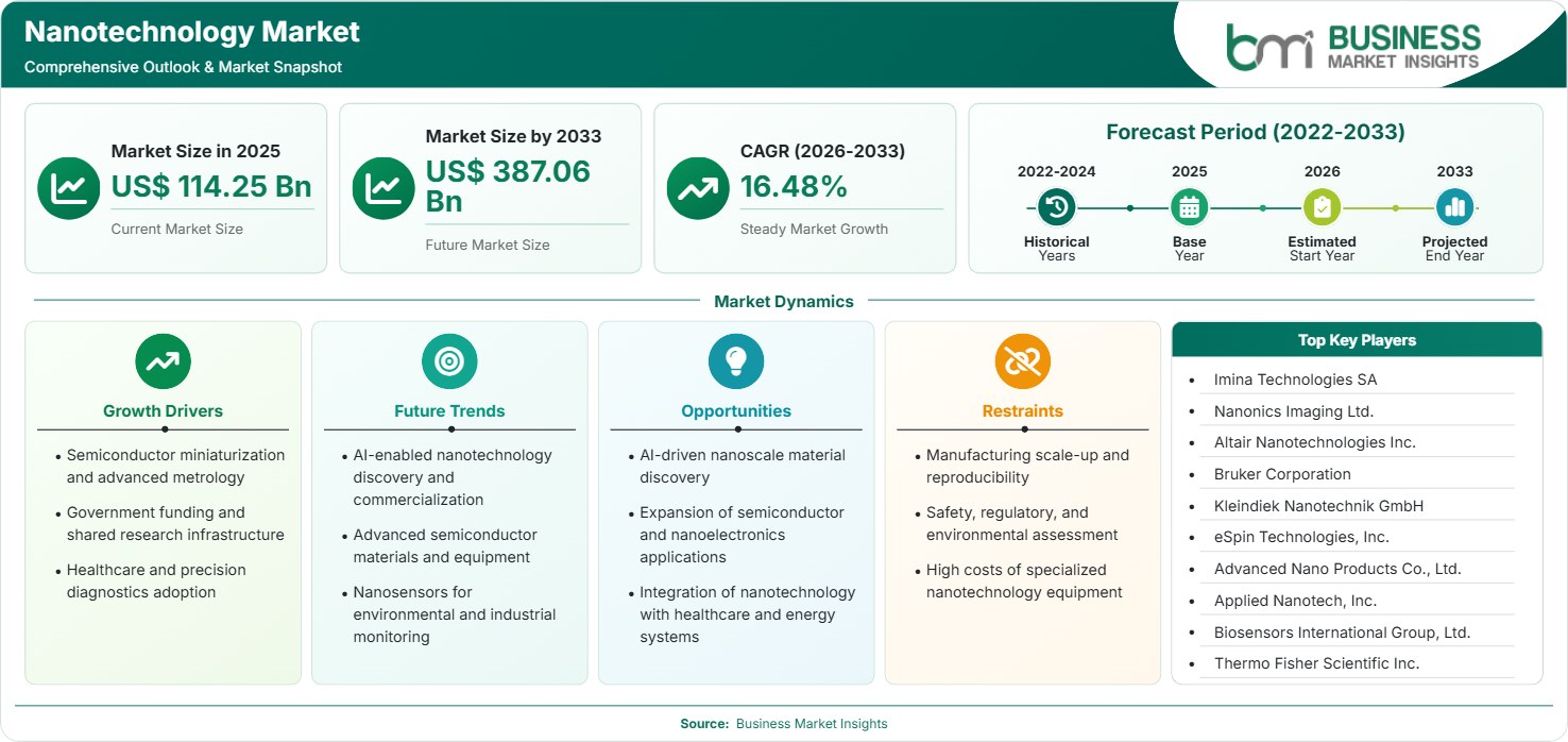
The Nanotechnology Market size was valued at US$ 114.25 Billion in 2025 and is projected to reach US$ 387.06 Billion by 2033, growing at a CAGR of 16.48% during 2026–2033, driven by semiconductor miniaturization, advanced healthcare, nanosensors, clean energy, precision manufacturing, and government-backed research.

Report Coverage
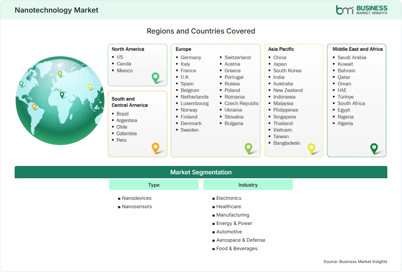
  • Type: Nanodevices, Nanosensors
  • Industry: Electronics, Healthcare, Manufacturing, Energy & Power, Automotive, Aerospace & Defense, Food & Beverages
US$ 114.25 Bn Market size in 2025
US$ 387.06 Bn Market Size by 2033
16.48% CAGR, 2026 - 2033
2026-2033 Forecast Period

AI Overview

Nanotechnology Market Summary

  • North America Region: North America holds a 28%–31% Nanotechnology Market share in 2025, growing with a 14%–16% CAGR, influenced by semiconductor research, biomedical innovation, defense programs, advanced characterization infrastructure, quantum technologies, and strong public-private R&D collaboration. The U.S. accounts for 69%–73% of North American demand, with a 14%–16% CAGR, supported by semiconductor fabrication, healthcare research, defense applications, and federal nanotechnology funding.
  • Fastest Growing Region: Asia Pacific holds a 30%–34% share of the Nanotechnology Market in 2025, growing with a 18%–20% CAGR, influenced by semiconductor manufacturing, electronics miniaturization, healthcare innovation, battery research, advanced materials, government incentives, and expanding nanotechnology commercialization programs.
  • Leading Segment: Nanodevices hold a 60%–64% share in 2025, growing with a 15%–17% CAGR, supported by semiconductor miniaturization, quantum technologies, nanoelectronics, advanced memory, medical devices, sensing systems, and increasing integration of nanoscale functionality into commercial products.
  • High Growth Segment: Nanosensors hold a 36%–40% share of the Nanotechnology Market in 2025, growing with a 18%–21% CAGR, driven by healthcare diagnostics, environmental monitoring, industrial process control, food safety, wearable devices, automotive sensing, and demand for highly selective, compact, low-power detection platforms.
  • Key Market Opportunity: Commercialization of nanosensors, quantum devices, nano-enabled medical diagnostics, advanced batteries, semiconductor materials, and intelligent manufacturing creates high-value opportunities for companies translating laboratory discoveries into scalable products.
  • Major Market Players: Imina Technologies SA, Nanonics Imaging Ltd., Altair Nanotechnologies Inc., Bruker Corporation, Kleindiek Nanotechnik GmbH, eSpin Technologies, Inc., Advanced Nano Products Co., Ltd., Applied Nanotech, Inc., Biosensors International Group, Ltd., and Thermo Fisher Scientific Inc.
Strategic Insights

Nanotechnology Market: Strategic Insights

Nanotechnology Market Strategic Framework
FREE PDF
Request your free sample
Request free sample
Stakeholder View

Key Takeaways

  • The ecosystem is becoming more integrated, linking nanomaterial developers, fabrication specialists, characterization-equipment suppliers, device manufacturers, healthcare companies, and semiconductor producers. Access to shared infrastructure remains important for reducing capital intensity and accelerating qualification.
  • Nanodevices provide the broadest commercial base, while nanosensors offer attractive incremental opportunities across diagnostics, environmental monitoring, industrial automation, food safety, automotive systems, and wearable electronics.
  • Research is moving toward multifunctional nanosystems that combine sensing, computation, actuation, and communication. Integration with artificial intelligence is also improving interpretation of complex nanoscale datasets and accelerating material discovery.
  • Asia Pacific presents a compelling investment case because semiconductor fabrication, electronics manufacturing, battery development, automotive production, and public R&D programs reinforce one another across several national ecosystems.
  • Public funding remains a major catalyst. The U.S. NNI has accumulated nearly US$47 billion in funding since 2001, while research infrastructure programs provide access to more than 2,000 advanced tools across participating NSF facilities.
  • Companies that convert laboratory-scale processes into reproducible manufacturing platforms can capture greater value than organizations focused exclusively on fundamental research, particularly where qualification barriers protect specialized applications.
Geographic Outlook

Nanotechnology Market Regional Highlights

North America Nanotechnology Market

North America held a 28%–31% share in 2025 and is projected to expand at a 14%–16% CAGR of the Nanotechnology Market through 2033. The region benefits from semiconductor R&D, biomedical research, aerospace programs, defense applications, quantum technology development, and sophisticated characterization infrastructure. The U.S. plays a dominant role in regional demand, whereas Canada is involved through advanced materials, biotech, and research institutions. Government involvement reduces the risks of technology development and commercialization. There are well-established venture capital systems in addition to university-industry partnerships for nanotech development.

  • Federal research programs continue supporting nanoscale science, with the 2026 NNI request allocating US$1.45 billion across participating agencies for foundational and application-oriented R&D.
  • Semiconductor research is strengthening demand for nanoprobing, electron microscopy, atomic force microscopy, defect analysis, and advanced metrology as device architectures become increasingly complex.
  • Healthcare laboratories are adopting nanoscale characterization for biomaterials, drug-delivery systems, diagnostics, and molecular research, expanding demand beyond conventional electronics applications.
  • Defense and aerospace programs provide opportunities for lightweight materials, advanced sensors, high-temperature components, electromagnetic materials, and radiation-resistant nanoscale technologies.

US Nanotechnology Market

The USA accounts for 69%–73% of North American market demand and is anticipated to register a 14%–16% CAGR through 2033. A diversified demand comes from federal agencies, universities, semiconductor producers, biotechnology organizations, and defense contractors. The National Nanotechnology Initiative unifies nanoscale research across government agencies, and the NSF infrastructure serves as a facility-sharing platform for collaboration between academia and industry. In addition, the USA Nanotechnology Market has an advantage in venture funding and semiconductor investment, creating commercialization pathways from laboratory discoveries to production-oriented nanodevices, sensors, materials, and analytical platforms.

  • The National Nanotechnology Coordinated Infrastructure connects 16 university-based facilities and provides access to more than 2,000 leading-edge tools, training resources, and technical expertise.
  • Albany NanoTech is strengthening the semiconductor ecosystem through public-private research programs and advanced process-development infrastructure, supporting demand for nanoscale metrology and characterization.
  • The U.S. healthcare ecosystem supports nanoscale research in drug delivery, diagnostics, biomaterials, imaging, and advanced medical-device development.

Europe Nanotechnology Market

Europe holds a 21%-24% market share in the Nanotechnology Market in 2025 and is expected to exhibit a 13%-15% CAGR during the period 2026-2033. Germany, France, the United Kingdom, the Netherlands, Switzerland, and the Nordic region have some important research and industrial competencies. Germany is an expert in manufacturing and instrumentation, whereas Switzerland is an expert in nanoprobing. France and the United Kingdom provide a good academic foundation and semiconductor research laboratories. The growth areas for Europe include frameworks for responsible development, advanced materials research, energy technology, innovation in health care, and safety testing of manufactured nanomaterials.

  • Germany remains a leading European market because industrial automation, advanced materials, semiconductor research, and scientific-instrumentation capabilities create sustained demand for nanoscale technologies.
  • Switzerland offers specialized opportunities in nanoprobing and semiconductor characterization, supported by companies such as Imina Technologies SA and advanced research institutions.
  • The European Union is strengthening responsible commercialization through updated guidance for manufactured nanomaterial safety testing released by the Joint Research Centre and OECD in December 2025.
  • The United Kingdom provides growth opportunities through semiconductor research, nanomaterials, biotechnology, and university-led commercialization programs.

Asia Pacific Nanotechnology Market

Asia Pacific accounted for 30% to 34% of overall demand in 2025 and is projected to grow at an 18% to 20% CAGR, making it the fastest-growing major region. The countries of interest within this region are China, Japan, South Korea, Taiwan, India, and Singapore. Demand from semiconductor fabrication, consumer electronics, batteries, automotive electronics, health care, and advanced materials occurs in parallel. South Korea is working to develop its semiconductor supply chain through new funding programs, while India is focusing on commercializing and integrating AI and nanotechnology into manufacturing processes.

  • China remains a major opportunity because electronics manufacturing, semiconductor investment, battery production, advanced materials, and research infrastructure provide multiple downstream routes for nanotechnology adoption.
  • South Korea is strengthening semiconductor materials, components, and equipment through a planned 5 trillion won industry fund, reinforcing opportunities for nanoscale materials and process technologies.
  • India is increasing commercialization activity, with Bengaluru INDIA NANO 2026 focusing on AI-nanotechnology convergence and translating research into practical applications.
  • Japan and Taiwan retain strong positions in precision electronics, semiconductor research, nanomaterials, instrumentation, and high-value component manufacturing.

Rest of World Nanotechnology Market

South and Central America Nanotechnology Market accounted for approximately 5%–7% within the Rest of World category in 2025, with the broader category projected to expand at a 12%–14% CAGR through 2033. Brazil and Mexico provide the strongest commercial opportunities, supported by healthcare, food processing, industrial manufacturing, mining, energy, and advanced materials research. Mexico additionally benefits from proximity to North American electronics and manufacturing supply chains.

Middle East and Africa represent emerging demand across energy, healthcare, environmental monitoring, food safety, and advanced materials. Saudi Arabia, the United Arab Emirates, Israel, and South Africa provide stronger technology-development ecosystems, while Gulf diversification programs can support investment in research infrastructure and specialized manufacturing.

  • Brazil offers opportunities in nanomedicine, agriculture, food safety, environmental sensing, and advanced materials, where nanoscale solutions can address resource-efficiency and monitoring requirements.
  • Mexico benefits from industrial integration with North American manufacturing, supporting demand for nanosensors, advanced coatings, electronic materials, and quality-control technologies.
  • Gulf economies are investing in technology diversification, creating opportunities for nanomaterials in energy storage, water treatment, environmental monitoring, healthcare, and industrial applications.
  • South Africa provides specialized opportunities through mining, environmental monitoring, healthcare research, and advanced materials applications requiring nanoscale characterization.
Global Market Geography
FREE PDF
Request your free sample
Request free sample
Segment Analysis

Nanotechnology Market Segmentation

Type

Nanodevices had a 60%-64% market share in 2025 and are expected to grow at a 15%-17% CAGR through 2033. Leadership is driven by applications such as semiconductor shrinkage, sensors, memory devices, quantum computing, and medicine. Nanosensor demand is growing faster because the healthcare industry, environmental sensing, automation, and wearable systems require increasingly selective detection at lower power and smaller physical dimensions.

  • Nanodevices: Nanodevices integrate nanoscale structures into functional electronic, optical, mechanical, and biomedical systems, benefiting from semiconductor miniaturization, quantum technologies, advanced memory, and compact medical-device architectures.
  • Nanosensors: Nanosensors exploit nanoscale surface, electrical, optical, or chemical properties for highly sensitive detection, supporting healthcare diagnostics, environmental monitoring, industrial automation, food safety, and wearable technologies.

Industry

Industry needs are technology-intensive and resource-sensitive, involving sectors such as electronics and medicine that offer avenues for commercialization. Others include energy and power, auto, aerospace and defense, and manufacturing. The scope of the Nanotechnology Market is growing as nanoscale materials and devices are being integrated into large-scale systems rather than remaining independent research products.

  • Electronics: Electronics uses nanotechnology for semiconductor components, conductive materials, memory, sensors, displays, quantum devices, and advanced packaging, with miniaturization and performance requirements accelerating adoption.
  • Healthcare: Healthcare applications include diagnostics, drug delivery, imaging, biomaterials, biosensors, and medical devices, where nanoscale engineering can improve targeting, sensitivity, surface properties, and device dimensions.
  • Manufacturing: Manufacturing applies nanomaterials, coatings, sensors, and precision characterization to improve durability, surface performance, process monitoring, defect detection, and production efficiency.
  • Energy & Power: Energy applications include batteries, fuel cells, solar technologies, catalysts, conductive materials, and energy-management sensors, where nanoscale structures can improve reaction efficiency and material performance.
  • Automotive: Automotive applications include nanosensors, lightweight materials, coatings, batteries, electronic components, and safety systems, supported by electrification, autonomous functions, and tighter packaging requirements.
  • Aerospace & Defense: Aerospace and defense use nanoscale materials and sensors for lightweight structures, thermal protection, surveillance, detection, communications, and high-performance components operating under demanding conditions.
  • Food & Beverages: Food applications include freshness sensing, contamination detection, packaging, barrier technologies, and ingredient engineering, with safety assessment and regulatory acceptance influencing commercialization pathways.
Market Forces

Nanotechnology Market Dynamics

Key Market Drivers

Semiconductor Miniaturization and Advanced Metrology

The need for nanoscale characterization in semiconductors is driven by the fact that transistors, interconnects, materials, and defects in these devices now operate at a scale where conventional inspection techniques fall short. Based on the findings of the Bruker 2025 report, atomic force microscopy enables characterization of semiconductor devices from the research and development stage to mass production, including surface roughness, defect inspection, critical-dimension analysis, and electrical, thermal, mechanical, and chemical properties. Similarly, Thermo Fisher recognizes electron microscopy as an important technique for characterizing future semiconductors. The above requirements have contributed to the market demand for nanoprobing, AFM, electron microscopy, sample preparation, and analytics. The Nanotechnology Market trends, therefore, increasingly favor integrated characterization workflows capable of linking nanoscale structure to electrical and chemical performance.

Government Funding and Shared Research Infrastructure

Government-funded nanotech research is also reducing the technical and economic barriers to implementing nanotechnology. The U.S. National Nanotechnology Initiative has requested a 2026 budget of US$1.45 billion and has received about US$47 billion in total since its formation. NSF's infrastructure facilities researchers provide academics, industry, and government scientists with access to over 2,000 instruments across 16 university-based facilities. Infrastructure facilities enable the discovery, manufacturing, measurement, biotechnology, and device fabrication of materials without requiring each company to develop its own laboratory infrastructure. Government investments foster collaboration between the university and industries and create specialized pools of talent.

Healthcare and Precision Diagnostics Adoption

Nanotechnology in healthcare can find applications due to the capabilities of nanoscale materials to enhance drug delivery systems, biosensors, imaging systems, and the surface modification of implants. For instance, the cardiovascular devices industry includes Biosensors International, which illustrates the commercial value of nanomaterials, as well as the NSF, which emphasizes applications of nanotechnology in medicine, diagnostics, and biology. The requirements in this industry call for developing a system that can detect lower biomarker concentrations and deliver more precise treatment. Thus, there are some possibilities for the development of nanosensors, nanoengineered surfaces, nanocomposites, and nanodiagnostic devices. However, commercialization will depend on clinical trials, reproducibility, biocompatibility, and regulatory approval.

Key Market Opportunities

AI-Enabled Nanotechnology Discovery and Commercialization

The use of artificial intelligence can help accelerate the development of nanotechnology through image processing during microscopy, the identification of relationships among material properties, parameter optimization, and structure prediction. Bengaluru, India, NANO 2026 understood very well the connection between AI and nanotech and how it could be commercially exploited. Areas of opportunity are material development, nanosensors, semiconductor defects, drug delivery, and optimization. AI can also make characterization more economical by identifying outliers in large datasets. Nanotechnology Market Forecasts will increasingly need to consider the intersection of these technologies because AI can expedite product development and increase reproducibility without any changes to the physical manufacturing process. Companies capable of linking data sets using customized algorithms can create strong intellectual property.

Advanced Semiconductor Materials and Equipment

The semiconductor sector offers one of the strongest commercialization opportunities because advanced chips require increasingly precise materials, deposition processes, inspection systems, and electrical characterization. The establishment of South Korea's 5 trillion-won investment in its semiconductor industry indicates how important the government considers domestic materials, components, equipment, and fabless technology. There are many areas where nanoscale suppliers can gain a competitive advantage, including conductive materials, coatings, nanoprobing, metrology, advanced packaging, and defect analysis tools. Other opportunities include future architectures such as chiplets, advanced memory, quantum components, and 3D integration. For suppliers that adhere to high process control requirements, qualification times are long and switching costs are high. Regional localization further supports investment in specialized manufacturing and research capabilities across Asia Pacific and North America.

Nanosensors for Environmental and Industrial Monitoring

Nanosensor technology can be used to solve monitoring problems that regular sensors cannot address due to insufficient sensitivity, selectivity, speed, or size. This includes monitoring environmental pollutants in water and air, exposure to chemicals and industrial emissions, process monitoring, leak detection, quality assurance, and predictive maintenance in the manufacturing industry, among others. Possible applications in the food industry include monitoring food freshness and detecting contamination. EFSA notes that the use of nanotechnology to detect the freshness of food packages has been studied. The most promising investment sectors are those in which the nanosensor operates continuously with low energy consumption and provides information to the monitoring system. The combination of nanosensors with wireless communication and machine learning interpretation would provide more valuable solutions than just a detection device.

Market Restraints and Challenges

Factor: Manufacturing Scale-Up and Reproducibility

Factor: Nanoscale materials and devices can exhibit performance differences caused by small changes in particle size, surface chemistry, morphology, deposition conditions, contamination, or process parameters.

Impact: laboratory results may not translate directly into high-volume production, increasing qualification costs and extending commercialization timelines. Reproducibility is particularly important in healthcare, electronics, and semiconductor applications where narrow specifications are required. Companies must invest in process controls, metrology, statistical monitoring, specialized equipment, and skilled personnel to maintain consistency. These requirements can increase capital expenditure and favor organizations with established manufacturing infrastructure. Shared research facilities reduce early-stage barriers, but commercial-scale production still requires dedicated process engineering and quality systems capable of controlling nanoscale variation throughout the value chain.

Factor: Safety, Regulatory, and Environmental Assessment

Factor: Manufactured nanomaterials can display physical and chemical behaviors that differ from their bulk counterparts, requiring specialized assessment of exposure, toxicity, environmental persistence, and lifecycle effects.

Impact: Additional testing requirements can increase development costs and delay market entry, particularly for food, healthcare, consumer, and environmental applications. European authorities and the OECD updated guidance in December 2025 covering sample preparation and dosimetry for safety testing of manufactured nanomaterials. Such frameworks improve confidence in responsible commercialization but also raise the technical documentation burden for manufacturers. Companies must therefore incorporate safety-by-design principles, standardized characterization, exposure assessment, and lifecycle evaluation early in development. Regulatory readiness can become a competitive advantage where customers prioritize traceability and predictable approval pathways.

Company Analysis

Competitive Landscape

The Nanotechnology Market analysis shows a fragmented competitive structure spanning scientific instrumentation, nanoprobing, nanomaterials, nanofibers, medical devices, nanosensors, and semiconductor characterization. Competitive differentiation increasingly depends on measurement precision, application expertise, intellectual property, manufacturing reproducibility, workflow integration, and access to specialized research ecosystems.

Company Name

Overview

Products and Services relevant to this market

Imina Technologies SA

Swiss manufacturer specializing in robotic micro- and nanoprobing solutions for semiconductor and research applications.

NANO nanoprobing platforms, microprobing systems, robotic positioning, electrical failure analysis, and Precisio software.

Nanonics Imaging Ltd.

Specialist microscopy company focused on scanning probe and near-field optical technologies for nanoscale research and characterization.

Near-field optical microscopes, scanning probe systems, nano-optical characterization, spectroscopy, and advanced imaging platforms.

Altair Nanotechnologies Inc.

U.S. nanotechnology company associated with advanced materials and nano-enabled energy and industrial applications.

Nanomaterials, advanced electrode materials, energy technologies, and specialized nanotechnology development solutions.

Bruker Corporation

Global analytical-instrumentation company with extensive AFM and nanoscale characterization capabilities serving research and industry.

Atomic force microscopes, nanoindentation, nanoIR, AFM probes, nanoscale metrology, and materials characterization.

Kleindiek Nanotechnik GmbH

German specialist providing high-precision nanoprobing and manipulation systems for electron microscopy environments.

Nanomanipulators, nanoprobing systems, in-situ TEM tools, electrical biasing equipment, and sample manipulation platforms.

eSpin Technologies, Inc.

U.S. nanofiber specialist focused on scalable electrospinning technologies and engineered nanofiber materials.

Nanofiber production systems, custom nanofiber media, filtration materials, research services, and engineered nanofiber solutions.

Advanced Nano Products Co., Ltd.

South Korean advanced-materials manufacturer supplying specialized nano-enabled materials for industrial and energy applications.

Conductive materials, silver pastes, nano-material solutions, photovoltaic materials, and advanced electronic-material products.

Applied Nanotech, Inc.

U.S. nanomaterials developer focused on electronics, sensors, energy, defense, and high-performance industrial applications.

Conductive inks, high-fidelity solders, printed superconductors, sensors, nanomaterial processes, and electronics packaging technologies.

Biosensors International Group, Ltd.

Singapore-headquartered medical-device company developing cardiovascular technologies and advanced drug-eluting stent platforms.

Drug-eluting stents, biomaterial technologies, cardiovascular devices, clinical systems, and specialty medical-device solutions.

Thermo Fisher Scientific Inc.

U.S. scientific-technology company providing advanced electron microscopy and nanoscale analytical workflows across research and industrial markets.

SEM, TEM, FIB-SEM, sample preparation, microscopy software, elemental analysis, semiconductor characterization, and nanotechnology research tools.

Trust & Transparency

Research Methodology

The market analysis combines proprietary research with secondary data from government agencies, company disclosures, regulatory filings, industry databases and expert interviews. Market estimates are validated through data triangulation, cross-market benchmarking and analyst review.

View Full Research Methodology

Questions Answered

Frequently Asked Questions

Where can businesses find the Nanotechnology Market Report insights most useful?

The report can support technology planning, regional expansion, competitive benchmarking, investment screening, product-development strategy, application prioritization, and partnership decisions. It is particularly relevant to companies evaluating nanodevices, nanosensors, advanced materials, scientific instrumentation, semiconductor technologies, healthcare applications, and emerging commercialization opportunities.

Why is responsible development important for nanoscale materials?

Nanoscale materials can behave differently from bulk substances because their surface area and physicochemical properties change at very small dimensions. Responsible development therefore requires appropriate exposure assessment, toxicity evaluation, lifecycle analysis, standardized characterization, and regulatory documentation before broad commercialization.

What role does nanotechnology play in energy storage?

Nanostructured electrodes, catalysts, conductive materials, coatings, and separators can modify electrochemical behavior and improve material utilization. Research is focused on batteries, fuel cells, hydrogen systems, solar technologies, and other energy platforms where surface area, transport properties, conductivity, and catalytic activity influence performance.

How does nanotechnology contribute to semiconductor manufacturing?

Nanotechnology supports advanced semiconductor manufacturing through nanoscale materials, process development, defect analysis, critical-dimension measurement, nanoprobing, advanced packaging, and characterization. These capabilities help manufacturers understand increasingly complex transistor structures, materials interfaces, interconnects, and failure mechanisms.

What technologies are most important for nanoscale characterization?

Atomic force microscopy, scanning electron microscopy, transmission electron microscopy, focused ion beam systems, nanoprobing, nanoindentation, spectroscopy, and advanced image-analysis software are central technologies. Their importance is increasing as semiconductor, materials, biological, and energy applications require simultaneous structural, electrical, chemical, and mechanical information.

Access the Full Nanotechnology Market Report

Get segment-level forecasts, regional estimates, competitive benchmarking, company profiles and downloadable Excel datasets.

Access the full Nanotechnology Market Report
350 pages PDF & Excel | 2026-08-27