
Cloud Eda Market Outlook: Size, Share, Trends, Growth Analysis, Competitive Landscape & Forecast, 2026-2033

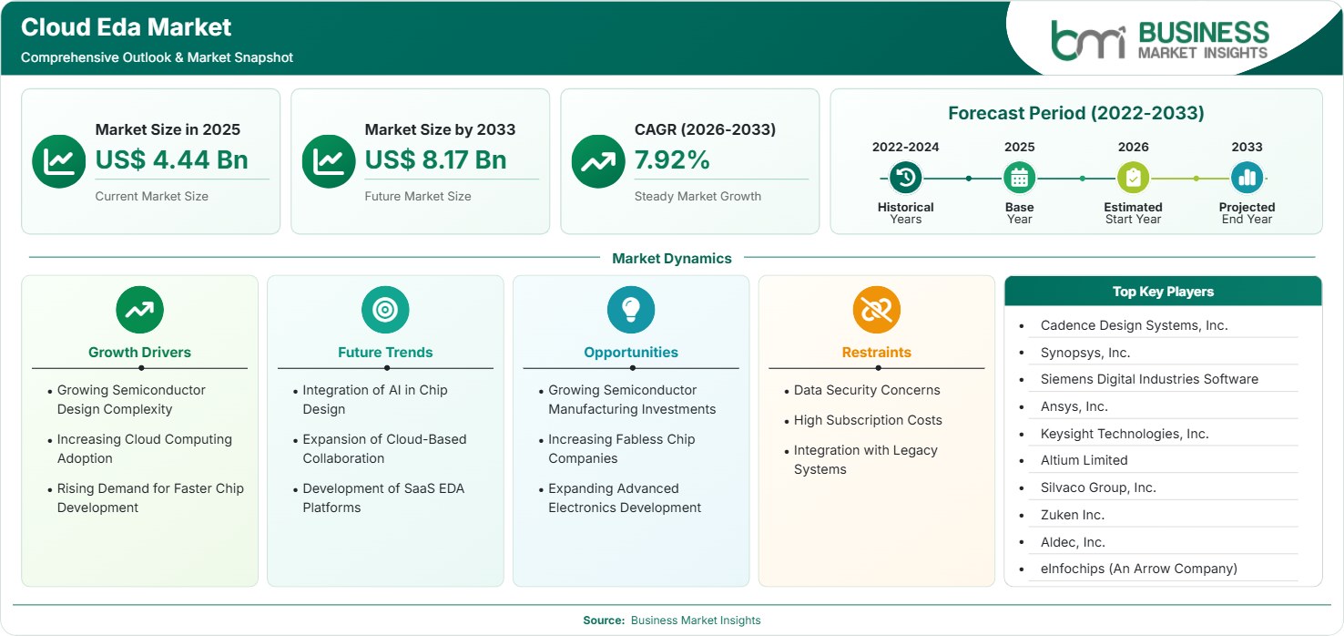
The Cloud EDA Market size was valued at US$ 4.44 Billion in 2025 and is projected to reach US$ 8.17 Billion by 2033, growing at a CAGR of 7.92% during 2026–2033, driven by semiconductor complexity, cloud-based collaboration, advanced chip development, and increasing demand for scalable electronic design solutions.

Report Coverage
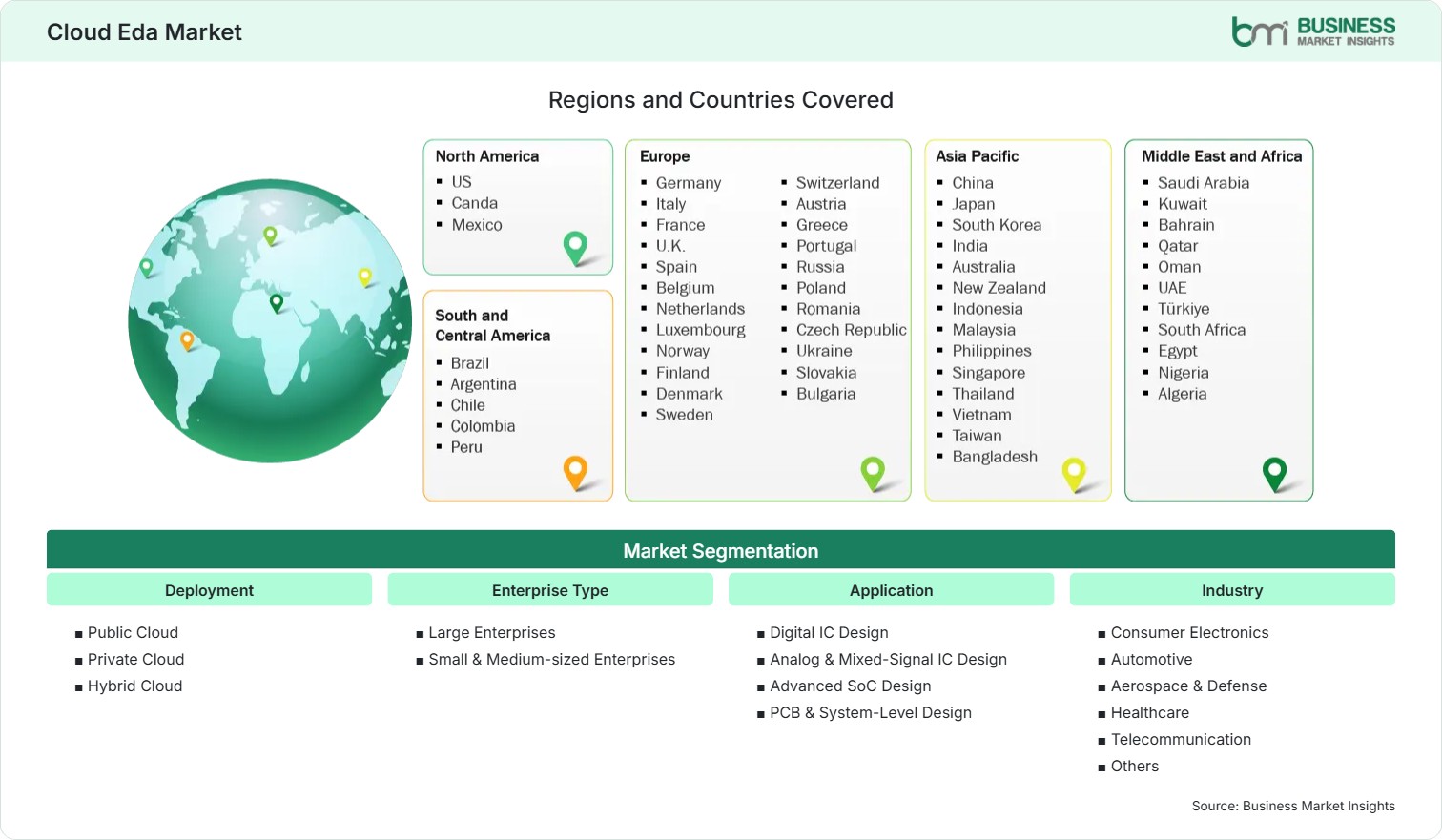
  • Deployment: Public Cloud, Private Cloud, Hybrid Cloud
  • Enterprise Type: Large Enterprises, Small & Medium-sized Enterprises
  • Application: Digital IC Design, Analog & Mixed-Signal IC Design, Advanced SoC Design, PCB & System-Level Design
  • Industry: Consumer Electronics, Automotive, Aerospace & Defense, Healthcare, Telecommunication, Others
US$ 4.44 Bn Market size in 2025
US$ 8.17 Bn Market Size by 2033
7.92% CAGR, 2026 - 2033
2026-2033 Forecast Period

01 AI Overview

Cloud Eda Market Summary

  • North America Region: North America holds a 35%–38% share in 2025, growing at a CAGR of 7.40%–8.10% through 2026–2033, supported by semiconductor innovation, AI chip development, cloud adoption, and advanced design infrastructure investments. The US market analysis indicates strong adoption with a CAGR of 7.50%–8.20% due to expanding fabless ecosystems, hyperscale computing investments, and semiconductor R&D activities.
  • Fastest Growing Region: Asia Pacific accounts for a 32%–35% share in 2025 and expands at a CAGR of 8.20%–8.90% during 2026–2033, supported by semiconductor manufacturing expansion, government incentives, growing electronics production, and increasing adoption of cloud-enabled engineering platforms.
  • Leading Segment: Private Cloud represents a 40%–43% share in 2025, advancing at a CAGR of 7.60%–8.20% during 2026–2033, driven by enterprise security requirements, intellectual property protection, controlled design environments, and semiconductor companies seeking customized cloud infrastructure.
  • High Growth Segment: Hybrid Cloud captures a 27%–30% share in 2025 and grows at a CAGR of 8.70%–9.30% during 2026–2033, fueled by flexible computing models, workload optimization, scalable simulation requirements, and integration of internal and external engineering resources.
  • Key Market Opportunity: Cloud-based electronic design platforms provide opportunities through distributed engineering, accelerated chip development cycles, AI-driven automation, and scalable computing access for emerging semiconductor companies worldwide.
  • Major Market Players: Cadence Design Systems, Inc.; Synopsys, Inc.; Siemens Digital Industries Software; Ansys, Inc.; Keysight Technologies, Inc.; Altium Limited; Silvaco Group, Inc.; Zuken Inc.; Aldec, Inc.; eInfochips (An Arrow Company).
02 Strategic Insights

Cloud Eda Market: Strategic Insights

Cloud Eda Market Strategic Framework
FREE PDF
Request your free sample
Request free sample
03 Stakeholder View

Key Takeaways

  • Semiconductor value chains are becoming increasingly interconnected, with EDA software providers, cloud infrastructure companies, chip designers, and foundries forming integrated ecosystems to support complex semiconductor development requirements.
  • High-growth opportunities are emerging from advanced SoC design, automotive semiconductor applications, and AI-focused chip development, where cloud computing resources help manage intensive simulation and verification workloads.
  • Innovation priorities are shifting toward AI-assisted design automation, machine learning-based verification, and scalable cloud architectures that improve productivity across semiconductor engineering teams.
  • Asia Pacific presents a strong investment opportunity due to semiconductor manufacturing expansion in countries such as China, South Korea, Taiwan, and India, supported by industrial policies and electronics supply chain development.
  • Strategic partnerships, technology integrations, and acquisitions among EDA providers and cloud technology companies are increasing as industry participants seek broader capabilities for semiconductor design workflows.
  • Enterprise adoption is being shaped by requirements for secure intellectual property management, flexible computing capacity, and faster development cycles across increasingly complex electronic systems.
04 Geographic Outlook

Cloud Eda Market Regional Highlights

North America Cloud EDA Market

North America maintains a leading position with a 35%–38% share in 2025 and records a CAGR of 7.40%–8.10% during 2026–2033. The region benefits from advanced semiconductor ecosystems, strong software capabilities, and high investments in AI, automotive electronics, and high-performance computing applications. Cloud EDA Market share remains concentrated among established technology providers and design-intensive enterprises. The United States contributes the largest regional demand, supported by semiconductor initiatives, research institutions, and increasing cloud infrastructure deployment across engineering organizations.

  • The United States continues attracting investments through semiconductor manufacturing incentives, expanding chip design activities, and increasing adoption of cloud-based engineering platforms among technology companies.
  • Leading EDA providers are strengthening partnerships with cloud infrastructure companies to deliver secure computing environments for advanced semiconductor design, verification, and simulation workloads.
  • Automotive semiconductor development and artificial intelligence hardware innovation are increasing demand for scalable design automation solutions across North American engineering teams.
  • Growing focus on domestic semiconductor supply chains is encouraging companies to modernize design infrastructure and adopt flexible cloud-based workflows.

US Cloud EDA Market

The US market accounts for a 30%–33% share in 2025 and expands at a CAGR of 7.50%–8.20% through 2026–2033. The country remains a central hub for semiconductor design, driven by established EDA companies, fabless semiconductor firms, and technology innovators. Cloud EDA Market growth in the US is supported by increasing computational requirements for advanced chip architectures, AI processors, and automotive electronics. Government initiatives supporting semiconductor development further strengthen domestic demand.

  • The presence of leading semiconductor designers and software developers creates a mature ecosystem for cloud-enabled electronic design automation adoption.
  • Increasing investments in artificial intelligence, data centers, and advanced computing applications are generating demand for faster chip design and verification capabilities.
  • Cloud-based platforms enable US enterprises to optimize engineering resources, improve collaboration, and reduce dependency on traditional hardware infrastructure.

Europe Cloud EDA Market

Europe represents a 20%–23% share in 2025 and grows at a CAGR of 7.10%–7.80% during 2026–2033. The region benefits from automotive semiconductor innovation, industrial automation development, and increasing investments in sovereign technology capabilities. Germany, France, and the United Kingdom are leading contributors, while countries developing semiconductor strategies are expanding adoption of advanced design platforms. Cloud EDA Market share is supported by automotive electronics manufacturers, research organizations, and semiconductor startups requiring efficient engineering environments.

  • Germany is advancing semiconductor design capabilities through automotive electronics demand, industrial automation applications, and investments in next-generation chip technologies.
  • France and the United Kingdom are supporting semiconductor innovation through research programs, advanced electronics development, and technology partnerships.
  • European automotive manufacturers are adopting cloud-enabled design solutions to accelerate development of electric vehicle and autonomous driving semiconductor systems.
  • Increasing focus on energy-efficient chip architectures is encouraging semiconductor companies to utilize advanced simulation and verification platforms.

Asia Pacific Cloud EDA Market

Asia Pacific holds a 32%–35% share in 2025 and records the fastest growth with a CAGR of 8.20%–8.90% during 2026–2033. The region benefits from semiconductor manufacturing dominance, expanding electronics production, and government-supported chip development initiatives. China, Taiwan, South Korea, Japan, and India are major contributors. Cloud EDA Market trends in Asia Pacific are influenced by increasing semiconductor investments, growing design complexity, and rising demand for scalable engineering solutions.

  • China is expanding semiconductor capabilities through domestic technology development programs and increasing adoption of advanced electronic design automation platforms.
  • Taiwan and South Korea continue driving demand through leading semiconductor manufacturing ecosystems and advanced process technology development.
  • India is emerging as a growing semiconductor design hub supported by engineering talent, digital infrastructure, and government technology initiatives.
  • Japan is strengthening semiconductor innovation through automotive electronics development and advanced manufacturing technology investments.

Rest of World Cloud EDA Market

Rest of World contributes a 7%–10% share in 2025 and expands at a CAGR of 6.80%–7.50% between 2026–2033. South and Central America are gradually adopting cloud-based engineering platforms as electronics manufacturing and technology investments increase. The Middle East and Africa are developing digital infrastructure and semiconductor-related capabilities through technology partnerships. Cloud EDA Market share remains smaller but demonstrates potential due to expanding innovation ecosystems and increasing demand for advanced electronics.

  • Brazil and Mexico are improving electronics manufacturing capabilities, creating opportunities for cloud-based semiconductor design and engineering solutions.
  • Middle Eastern countries are investing in digital transformation initiatives that support advanced technology adoption and semiconductor ecosystem development.
  • African technology hubs are increasing demand for scalable design platforms through growing electronics and innovation sectors.
  • Regional partnerships with global technology providers are improving access to advanced semiconductor design capabilities.
  • Increasing cloud infrastructure availability is supporting adoption among emerging engineering organizations seeking cost-effective design environments.
Global Market Geography
FREE PDF
Request your free sample
Request free sample
05 Segment Analysis

Cloud Eda Market Segmentation

Deployment

Deployment represents a critical segmentation factor, with private cloud leading adoption due to semiconductor companies prioritizing security, intellectual property protection, and controlled computing environments. The segment accounts for a 40%–43% share in 2025 and grows at a CAGR of 7.60%–8.20% between 2026–2034. The Cloud EDA Market scope expands as enterprises balance performance, scalability, and cybersecurity requirements through flexible deployment models.

  • Public Cloud: Public cloud platforms provide scalable computing resources for semiconductor design teams requiring flexible access, reduced infrastructure investment, and efficient workload management across distributed engineering environments.
  • Private Cloud: Private cloud solutions support sensitive semiconductor projects by offering enhanced security, customized infrastructure, and dedicated computing resources for complex design and verification operations.
  • Hybrid Cloud: Hybrid cloud adoption increases as organizations combine internal infrastructure with external cloud resources to optimize performance, security, and computational flexibility for advanced semiconductor workflows.

Enterprise Type

Enterprise type segmentation reflects adoption differences between large semiconductor organizations and smaller technology companies. Large enterprises maintain a leading position due to complex design requirements, extensive engineering teams, and higher cloud investment capacity. The segment represents a 55%–58% share in 2025 with a CAGR of 7.50%–8.10% through 2026–2034. SMEs are increasingly adopting cloud solutions to access advanced capabilities without major infrastructure expenses.

  • Large Enterprises: Large enterprises utilize cloud EDA platforms for complex chip development, global collaboration, advanced verification processes, and integration with existing semiconductor engineering workflows.
  • Small & Medium-sized Enterprises (SMEs): SMEs adopt cloud-based solutions to reduce capital requirements, access advanced design tools, and accelerate product development through scalable computing environments.

Application

Application segmentation highlights increasing demand across advanced semiconductor development areas. Advanced SoC Design represents a significant portion with a 30%–33% share in 2025 and CAGR of 8.20%–8.80% during 2026–2034. Growing chip complexity, AI applications, and connected devices are strengthening adoption across multiple design categories. Cloud EDA Market trends indicate rising integration of simulation, verification, and automation capabilities.

  • Digital IC Design: Digital IC design applications benefit from increasing demand for processors, memory solutions, and advanced computing chips requiring efficient verification and simulation capabilities.
  • Analog & Mixed-Signal IC Design: Analog and mixed-signal design adoption grows through automotive, industrial, and communication applications requiring accurate modeling and performance optimization.
  • Advanced SoC Design: Advanced SoC design platforms support complex semiconductor architectures by enabling scalable computation, faster verification, and improved collaboration among global engineering teams.
  • PCB & System-Level Design: PCB and system-level design applications expand through electronic product innovation, connected devices, and increasing system integration requirements.
06 Market Forces

Cloud Eda Market Dynamics

Key Market Drivers

Growing Semiconductor Design Complexity

Higher transistor density, small process nodes, and sophisticated chip designs are boosting the demand for sophisticated design automation platforms. The semiconductor industry is still heading towards smaller process geometries and heterogeneous integration; therefore, there is a necessity of comprehensive simulation and verification features. The growth of market is driven by the increasing demand for computing infrastructure which can handle the large volume of design data sets. It is expected that the Cloud EDA market trends will witness growing demand from organizations designing AI processors, automotive chips, and high-performance computing systems. Modern design methodologies need sophisticated infrastructure for handling compute-intensive operations, thus helping in lowering the time-to-market and boosting productivity.

Increasing Cloud Computing Adoption

Cloud computing in semiconductor engineering companies is changing the way design teams use computational power and collaborate globally and handle work processes. The semiconductor companies are switching from the conventional infrastructure systems to scalable cloud systems which offer more flexibility and efficient management of operations. With the increased number of secure cloud systems, the semiconductor firms will be able to conduct simulations without having to have large physical infrastructures. Growth of the Cloud EDA Market is enhanced through enterprises looking for resource optimization, cost reduction, and quick acquisition of computing power.

Rising Demand for Faster Chip Development

The rapid cycles of innovations in semiconductors lead to increased demands for EDA tools which will help reduce development times. Companies in automotive industry, telecommunications, artificial intelligence, and consumer electronics need to introduce chips faster in order to preserve competitive advantage. Cloud design platforms can help organizations achieve faster verification, automate routine activities, and address the problem of growing engineering complexity. The trends in Cloud EDA Market indicate the growing preference for products combining automation, high performance, and collaboration. The semiconductor companies are competing to develop advanced processors and specialized chips, and cloud environment offers the necessary flexibility to do so.

Key Market Opportunities

Growing Semiconductor Manufacturing Investments

Increasing investments in semiconductor manufacturing facilities create opportunities for cloud-based electronic design automation providers by expanding demand for advanced design capabilities. The construction of new fabrication facilities necessitates efficient engineering eco-systems that aid the development, testing, and optimization of the chip. Semiconductor initiatives by government in regions such as North America, Europe, and Asia-Pacific are pushing the investment in the entire semiconductor supply chain. The Cloud EDA market forecast indicates the likelihood of increased adoption potential due to the need by manufacturers and design firms for platforms to enhance their next-generation technologies. The emergence of advanced nodes, artificial intelligence chips, and automotive semiconductors provides more room for cloud-based design platforms.

Increasing Fabless Chip Companies

The expansion of fabless semiconductor companies is creating new demand for cloud-based EDA solutions that provide access to advanced design capabilities without significant infrastructure investments. Small semiconductor developers now utilize cloud platforms in order to handle complicated workflows, perform simulations, and collaborate with other players from outside the company. The emergence of special chips for the purposes of artificial intelligence, edge computing, and automotive industry leads to the situation when more organizations decide to join the market of semiconductors design. Cloud technology gives the possibility to compete with others in such an environment because of availability of computing power and software tools.

Expanding Advanced Electronics Development

Growth in advanced electronics applications is creating opportunities for cloud EDA providers across industries such as automotive, healthcare, telecommunications, and aerospace. Connected devices, autonomous systems, and high-performance computing applications require increasingly complex semiconductor architectures. Cloud platforms enable engineering teams to manage sophisticated design requirements while improving collaboration efficiency. Future adoption opportunities are emerging through integration of artificial intelligence, machine learning, and automation capabilities within design workflows. Companies investing in next-generation electronic systems are increasingly seeking flexible solutions that support faster development cycles and improved product performance. This creates a favorable environment for cloud-enabled EDA technologies across diverse application segments.

Market Restraints and Challenges

Data Security Concerns

Factor: Increasing concerns regarding intellectual property protection and unauthorized access to sensitive semiconductor designs impact enterprise willingness to migrate critical workloads to cloud environments. Impact: Companies with highly confidential chip architectures may delay adoption due to cybersecurity risks and compliance requirements. Semiconductor designs contain valuable proprietary information, making secure data management essential for cloud EDA deployment. Although providers are improving encryption, access controls, and compliance frameworks, security considerations remain a major evaluation factor. Organizations must balance cloud scalability benefits with protection requirements. Strong cybersecurity infrastructure, industry standards, and trusted cloud partnerships will influence adoption rates among semiconductor companies handling sensitive design data.

High Subscription Costs

Factor: Premium pricing structures associated with advanced cloud EDA software subscriptions can increase operational expenses for smaller organizations and emerging semiconductor companies. Impact: Higher software costs may limit adoption among SMEs with restricted technology budgets. Advanced simulation, verification, and automation capabilities require continuous investment in software licenses, cloud computing resources, and technical expertise. Companies must evaluate cost benefits against productivity improvements and reduced infrastructure requirements. While cloud models reduce upfront hardware investments, recurring subscription expenses remain a challenge for budget-sensitive users. Flexible pricing models, usage-based billing, and scalable service packages could help improve accessibility across different enterprise categories.

07 Company Analysis

Competitive Landscape

The Cloud EDA Market analysis highlights a competitive ecosystem where global EDA providers focus on cloud integration, semiconductor design automation, simulation capabilities, and strategic technology partnerships. Leading companies are enhancing platforms to support advanced semiconductor architectures, AI-driven workflows, and distributed engineering operations.

Company Name

Overview

Products and Services relevant to this market

Cadence Design Systems, Inc.

Cadence provides electronic design automation solutions supporting semiconductor development, verification, and system innovation across multiple industries.

Cloud-based EDA platforms, digital design tools, verification solutions, and semiconductor engineering workflows.

Synopsys, Inc.

Synopsys delivers semiconductor design and verification technologies used by global chip developers and technology companies.

Cloud EDA services, chip design automation, verification platforms, and semiconductor IP solutions.

Siemens Digital Industries Software

Siemens provides digital engineering software supporting electronics design, simulation, and industrial technology development.

Cloud-enabled EDA solutions, PCB design, simulation tools, and integrated engineering platforms.

Ansys, Inc.

Ansys develops simulation software supporting engineering analysis across electronics and semiconductor applications.

Semiconductor simulation tools, electronic analysis platforms, and cloud-based engineering solutions.

Keysight Technologies, Inc.

Keysight delivers electronic design and testing technologies for communication and semiconductor industries.

Design simulation, validation platforms, measurement software, and cloud-enabled engineering solutions.

Altium Limited

Altium specializes in PCB design software supporting electronic product development and collaboration.

Cloud-based PCB design platforms, collaboration tools, and electronic development environments.

Silvaco Group, Inc.

Silvaco provides semiconductor design software supporting technology development and device modeling.

TCAD simulation, semiconductor modeling tools, and cloud-compatible design solutions.

Zuken Inc.

Zuken develops electronic design software for automotive, industrial, and electronics applications.

PCB design automation, electrical engineering tools, and collaborative design platforms.

Aldec, Inc.

Aldec provides electronic design verification solutions focused on semiconductor development efficiency.

FPGA verification tools, simulation platforms, and design automation technologies.

eInfochips (An Arrow Company)

eInfochips provides engineering services and semiconductor solutions supporting digital transformation initiatives.

Semiconductor design services, embedded systems solutions, and cloud engineering support.

10 Trust & Transparency

Research Methodology

The market analysis combines proprietary research with secondary data from government agencies, company disclosures, regulatory filings, industry databases and expert interviews. Market estimates are validated through data triangulation, cross-market benchmarking and analyst review.

View Full Research Methodology

11 Questions Answered

Frequently Asked Questions

What factors influence the adoption of the Cloud EDA Market Report insights?

The report insights are influenced by semiconductor investment cycles, technology advancements, cloud infrastructure development, design complexity, and increasing demand for efficient electronic engineering solutions.

What security measures support enterprise adoption of cloud EDA?

Cloud EDA providers are implementing encryption technologies, identity management systems, compliance frameworks, and controlled access mechanisms to protect sensitive semiconductor designs and intellectual property during digital engineering workflows.

Why are fabless semiconductor companies adopting cloud EDA platforms?

Fabless companies use cloud EDA platforms to access advanced design capabilities while reducing infrastructure investment requirements. These solutions allow smaller organizations to compete by improving engineering efficiency and supporting complex chip development processes.

What industries are driving demand for cloud-based EDA solutions?

Automotive, artificial intelligence, telecommunications, consumer electronics, and aerospace industries are major contributors due to increasing semiconductor integration requirements and demand for specialized chips with improved performance capabilities.

How does cloud adoption change semiconductor design workflows?

Cloud adoption enables semiconductor teams to access scalable computing resources, collaborate across locations, and execute complex simulations without maintaining extensive physical infrastructure. It improves flexibility for design verification and advanced chip development activities.

Access the Full Cloud Eda Market Report

Get segment-level forecasts, regional estimates, competitive benchmarking, company profiles and downloadable Excel datasets.

Access the full Cloud Eda Market Report
350 pages PDF & Excel | 2026-08-07