
Wafer Level Packaging Market Outlook: Size, Share, Trends, Growth Analysis, Competitive Landscape & Forecast, 2026-2033

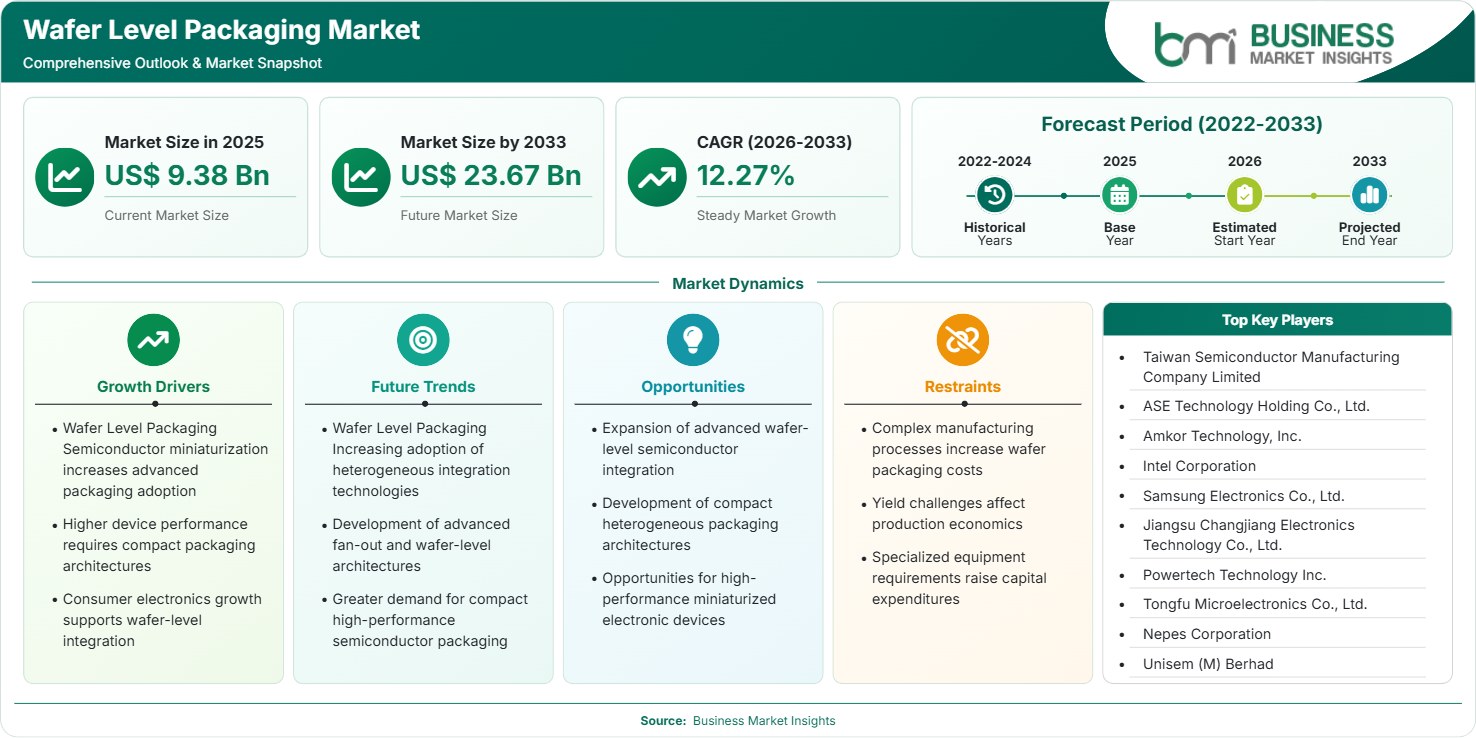
The Wafer Level Packaging Market size was valued at US$ 9.38 Billion in 2025 and is projected to reach US$ 23.67 Billion by 2033, growing at a CAGR of 12.27% during 2026–2033, driven by AI computing, heterogeneous integration, miniaturization, automotive electronics, advanced connectivity, and chiplet adoption.

Report Coverage
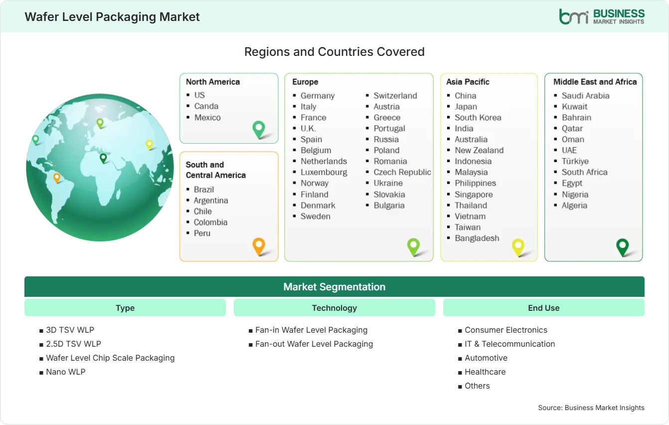
  • Type: 3D TSV WLP, 2.5D TSV WLP, Wafer Level Chip Scale Packaging, Nano WLP
  • Technology: Fan-in Wafer Level Packaging, Fan-out Wafer Level Packaging
  • End Use: Consumer Electronics, IT & Telecommunication, Automotive, Healthcare, Others
US$ 9.38 Bn Market size in 2025
US$ 23.67 Bn Market Size by 2033
12.27% CAGR, 2026 - 2033
2026-2033 Forecast Period

AI Overview

Wafer Level Packaging Market Summary

  • North America Region: North America holds a 22%–25% Wafer Level Packaging Market share in 2025, growing at a 10.8%–11.6% CAGR, supported by AI infrastructure, semiconductor localization, defense electronics, advanced foundry investment, automotive computing, and high-performance packaging requirements. The US represents 78%–82% of regional demand, expanding at a 10.5%–11.3% CAGR through 2033 as domestic advanced packaging, AI infrastructure, and defense semiconductor investment accelerates.
  • Fastest Growing Region: Asia Pacific holds a 49%–53% share in 2025, expanding at a 13.0%–14.0% CAGR, supported by foundry investment, OSAT expansion, mobile electronics, AI accelerators, automotive semiconductors, memory production, and increasingly localized semiconductor supply chains.
  • Leading Segment: Fan-out Wafer Level Packaging (FO-WLP) holds a 43%–47% share in 2025, advancing at a 13.0%–14.0% CAGR, supported by higher I/O density, thinner form factors, substrate reduction, heterogeneous integration, mobile processors, networking devices, and chiplet architectures.
  • High Growth Segment: 3D TSV WLP holds a 10%–13% Wafer Level Packaging Market share in 2025 and is advancing at a 14.5%–15.5% CAGR, driven by vertical integration, HBM proximity, chiplet architectures, shorter interconnects, AI accelerators, high-bandwidth computing, and advanced thermal management requirements.
  • Key Market Opportunity: Expansion of fan-out, TSV, chiplet, and panel-level architectures creates opportunities across AI, automotive computing, optical networking, edge devices, healthcare electronics, and high-density communications.
  • Major Market Players: Taiwan Semiconductor Manufacturing Company Limited; ASE Technology Holding Co., Ltd.; Amkor Technology, Inc.; Intel Corporation; Samsung Electronics Co., Ltd.; Jiangsu Changjiang Electronics Technology Co., Ltd.; Powertech Technology Inc.; Tongfu Microelectronics Co., Ltd.; Nepes Corporation; Unisem (M) Berhad.
Strategic Insights

Wafer Level Packaging Market: Strategic Insights

Wafer Level Packaging Market Strategic Framework
FREE PDF
Request your free sample
Request free sample
Stakeholder View

Key Takeaways

  • Supply-chain value is shifting toward integrated ecosystems connecting foundries, OSATs, substrate suppliers, materials companies, equipment manufacturers, design houses, and semiconductor customers.
  • Fan-out packaging provides the strongest commercial upside because it combines thin profiles, expanded routing, heterogeneous integration, and substrate reduction across consumer, automotive, networking, and computing applications.
  • Advanced RDL, TSV, hybrid bonding, embedded bridges, and chiplet integration are converging, allowing semiconductor designers to optimize package-level bandwidth, thermal behavior, and power delivery.
  • Taiwan remains a compelling investment geography because foundries, OSATs, materials suppliers, equipment companies, and semiconductor designers operate within a highly integrated production ecosystem.
  • Investment is moving toward automation, larger-format processing, advanced inspection, panel-level manufacturing, and geographically diversified capacity as package complexity rises.
  • M&A and strategic partnerships are becoming more important because successful package qualification requires coordinated expertise in materials, process engineering, reliability, testing, thermal management, and design.
Geographic Outlook

Wafer Level Packaging Market Regional Highlights

North America Wafer Level Packaging Market

North America accounts for a 22%–25% share in 2025 and is projected to expand at a 10.8%–11.6% CAGR through 2033. The regional ecosystem is concentrated in the United States, where AI accelerators, defense electronics, networking, automotive computing, and domestic semiconductor investment support advanced packaging localization. The Wafer Level Packaging Market share reflects strong demand for high-performance integration, while the Market growth profile increasingly depends on domestic capacity, qualified suppliers, and strategic semiconductor manufacturing programs.

  • AI infrastructure is driving increasing demand for high-density packages, advanced interconnects, and thermally efficient architectures across accelerator, processor, and networking platforms.
  • Defense semiconductor programs are strengthening demand for trusted domestic packaging and improving the strategic importance of traceable backend manufacturing capacity.
  • US foundry expansion is encouraging greater proximity among wafer fabrication, advanced packaging, semiconductor testing, materials suppliers, and chip design ecosystems.
  • Canada and Mexico provide complementary electronics manufacturing capabilities, although advanced wafer-level capacity remains concentrated in the United States.

US Wafer Level Packaging Market

The US Wafer Level Packaging Market represents 78%–82% of North American demand in 2025 and is forecast to grow at a 10.5%–11.3% CAGR. Domestic semiconductor localization, AI infrastructure, defense electronics, and advanced foundry strategies are strengthening demand. The country combines major semiconductor design centers with expanding manufacturing capabilities, creating opportunities for integrated packaging ecosystems. Demand is increasingly oriented toward high-performance computing, automotive electronics, networking, and secure semiconductor supply chains rather than commodity packaging alone.

  • Arizona and New Mexico are emerging as important semiconductor manufacturing nodes, linking leading-edge wafer production with domestic packaging and system integration capabilities.
  • Defense programs are increasing qualification demand for trusted semiconductor manufacturing where traceability, security, and supply-chain control influence procurement decisions.
  • Silicon Valley remains a major semiconductor design center, supporting packaging innovation through collaboration among designers, EDA companies, foundries, and OSAT providers.

Europe Wafer Level Packaging Market

Europe represents a 16%–19% share in 2025 and is expanding at a 10.2%–11.0% CAGR. Germany remains the leading automotive semiconductor ecosystem, while France and the Netherlands provide important semiconductor technology, photonics, and equipment capabilities. Germany is positioned at 10.5%–11.3% CAGR and France at 11.0%–12.0%, supported by automotive electrification, industrial automation, communications, and semiconductor localization. The Wafer Level Packaging Market share is increasingly influenced by reliability requirements and high-value industrial applications.

  • Germany benefits from automotive semiconductor demand, supporting wafer-level packaging for sensors, radar, power management, and vehicle computing applications.
  • France is strengthening semiconductor and photonics capabilities, creating opportunities for compact packages serving communications, industrial systems, and edge computing.
  • The Netherlands remains strategically important through semiconductor equipment capabilities, indirectly supporting advanced packaging development and process innovation.
  • Automotive qualification standards favor packages capable of consistent thermal cycling, moisture resistance, mechanical reliability, and extended product lifecycles.

Asia Pacific Wafer Level Packaging Market

Asia Pacific holds a 49%–53% share in 2025 and is projected to grow at a 13.0%–14.0% CAGR, making it the largest and fastest-growing regional market. Taiwan remains the leading production center, while South Korea, China, Japan, and Southeast Asia contribute expanding capacity. Taiwan is positioned at 13.5%–14.5% CAGR, and South Korea near 12.5%–13.5%. The Wafer Level Packaging Market growth profile reflects strong foundry, memory, mobile, automotive, and OSAT investment.

  • Taiwan benefits from dense foundry and OSAT ecosystems, particularly for fan-out, 2.5D, 3D, and heterogeneous integration applications.
  • South Korea is advancing fan-out and panel-level packaging alongside memory and mobile processor production, creating cross-segment integration opportunities.
  • China is expanding domestic semiconductor packaging capacity, targeting automotive, consumer electronics, communications, and computing applications.
  • Southeast Asia is gaining importance as multinational manufacturers diversify assembly and testing footprints across Malaysia, Singapore, and the Philippines.

Rest of World Wafer Level Packaging Market

South and Central America Wafer Level Packaging Market maintains smaller demand pools, with Brazil and Mexico providing the strongest electronics manufacturing foundations. The regional market is projected to expand at an 8.5%–9.5% CAGR, supported by automotive, telecommunications, industrial electronics, and consumer devices. Mexico benefits from integration with North American production networks, while Brazil provides a broader domestic electronics base. Advanced packaging capacity remains more limited than in Asia Pacific, creating opportunities for specialized services and supply-chain partnerships.

The Middle East and Africa are forecast to experience demand growth at a CAGR of 9.0%–10.0%, driven by the UAE, Saudi Arabia, Israel, and certain African technology hubs. The demand is associated with the infrastructure of artificial intelligence, telecommunications, defense, automotive, and digital transformation. Israel boasts the best semiconductor design ecosystem, whereas the Gulf States are developing their capabilities in technology and data centers.

  • Mexico provides the strongest connection to North American electronics production, particularly across automotive and industrial semiconductor supply chains.
  • Brazil supports semiconductor demand through domestic industrial applications, consumer electronics, telecommunications, automotive production, and embedded systems.
  • Israel provides a technology-intensive semiconductor design ecosystem supporting advanced computing, communications, defense, and specialized electronics applications.
  • Gulf states are increasing digital infrastructure investment, creating opportunities linked to AI, telecommunications, data centers, automotive technology, and electronics localization.
Global Market Geography
FREE PDF
Request your free sample
Request free sample
Segment Analysis

Wafer Level Packaging Market Segmentation

Type

The Type segment is shaped by increasing integration density, miniaturization, and heterogeneous computing requirements. Fan-out and WLCSP remain important volume architectures, while Wafer Level Packaging Market scope TSV-based packages address advanced integration. The category is projected to advance at approximately 12%–14% through 2033 as package-level functionality becomes more important across computing, mobile, automotive, and communications applications.

  • 3D TSV WLP: Vertical interconnection supports compact stacking and high bandwidth, serving HBM, AI accelerators, memory-intensive processors, and chiplet architectures requiring short signal paths.
  • 2.5D TSV WLP: Interposer-based integration supports multi-die architectures and high routing density for processors, accelerators, and memory-intensive systems.
  • Wafer-Level Chip Scale Packaging (WLCSP): WLCSP supports PMICs, sensors, RF devices, and connectivity ICs by minimizing package dimensions, materials, and electrical path length.
  • Nano WLP: Nano-scale redistribution and ultra-thin concepts target wearables, sensors, miniaturized electronics, and specialized devices where package dimensions constrain system design.

Technology

The use of technology now creates a division between high-volume fan-in technology and more integrated fan-out technology. The fan-out facilitates routing the connection outside the die. This kind of technology is expected to grow at around 13% - 15% due to the connectivity needs of mobile, AI, automotive, networking, and chiplet technologies.

  • Fan-in Wafer-Level Packaging (FI-WLP): FI-WLP remains cost-efficient for compact dies with adequate pad areas, supporting PMIC, analog, RF, sensor, and connectivity applications.
  • Fan-out Wafer-Level Packaging (FO-WLP): FO-WLP expands routing beyond die boundaries, enabling thinner packages, higher density, heterogeneous integration, substrate reduction, and flexible system architectures.

End Use

The end-use demand reflects the increasing importance of packaging to the system's performance. The consumer electronics segment offers high volumes, whereas the automotive and healthcare segments focus on reliability. IT and telecommunications are more concerned with bandwidth and thermal efficiency. Industrial and military electronic products drive demand for value-added packaging systems.

  • Consumer Electronics: Smartphones, wearables, tablets, and connected devices favor thin, lightweight packages with high electrical performance, supporting WLCSP and fan-out adoption.
  • IT & Telecommunication: Data centers, networking equipment, optical systems, and communications infrastructure require high-density interconnects, thermal efficiency, and multi-die integration.
  • Automotive: Electrification, ADAS, radar, centralized computing, and vehicle networking increase demand for reliable packages with stronger thermal and mechanical performance.
  • Healthcare: Imaging, diagnostics, monitoring, and portable medical electronics require compact, reliable semiconductor packages with controlled power consumption and integration flexibility.
  • Others: Industrial automation, aerospace, defense, energy systems, and specialized electronics provide additional demand where reliability, form factor, and long lifecycle requirements support advanced packaging.
Market Forces

Wafer Level Packaging Market Dynamics

Key Market Drivers

AI and Heterogeneous Integration

AI accelerators are increasing package requirements for bandwidth, power delivery, thermal management, and die-to-die connectivity. 3D Stacking, advanced redistribution, and high-density integration enable shorter signal lengths and higher functionality density within limited package footprints. This type of packaging becomes especially important for AI chips that integrate Logic, high-bandwidth memory, Networking, and Accelerators. As a result, the Wafer Level Packaging Market growth depends on package complexity rather than on semiconductor units alone. Suppliers capable of managing warpage, fine-line redistribution, bonding precision, thermal management, and yield can tap into high-value-added markets. Such Market trends show a move towards package optimization along with chip architecture, node technology, memory, and power delivery planning.

Mobile and Connectivity Miniaturization

Further reductions in package thickness will be required for future smartphones, wearables, RF components, and electronics without any decrease in I/O density or performance. WLCSP continues to work well for small-form-factor devices, and fan-out enables routing when normal die sizes restrict routing options. Mobile CPUs continue to become more complex and must be packaged to meet power delivery, thermal performance, and signal integrity requirements within limited space. This evolution helps make wafer-level technology more prevalent in high-end consumer electronics and connectivity solutions. Thus, Wafer Level Packaging Market trends will include a need for reduced thickness, greater functionality, shorter electrical paths, and higher manufacturing yield.

Automotive Electronics Electrification

The content of semiconductors in automobiles is growing due to ADAS, car networking, electrification, radars, sensors, and computing systems. The packaging needs to withstand thermal cycles, mechanical stress, moisture, vibration, and long-lifetime cycles. This means that suppliers who have expertise in process control, materials science, and reliability testing will benefit. Advanced packaging solutions will reduce interconnects and increase functionality. Wafer-level architectures are therefore moving beyond traditional consumer applications into higher-value automotive systems where qualification requirements create stronger barriers to entry. Automotive demand also provides greater visibility because semiconductor programs often have longer product lifecycles than mobile electronics. The Wafer Level Packaging Market forecast opportunity is consequently supported by increasing semiconductor content per vehicle and the migration toward software-defined vehicle architectures.

Key Market Opportunities

Panel-Level Processing Expansion

The possibility of panel-level processing allows scaling up wafer fabrication economics to apply them to larger packages, in addition to improving manufacturing area utilization. With more space available on the processing surface, the number of packages manufactured per production cycle could increase, and there is also room to improve material utilization. The possibilities are especially interesting for artificial intelligence (AI) and high-performance computing (HPC) packages that are getting larger. But commercial viability will depend on solving issues with warpage, alignment, lithography, molding, carrier handling, and yield. Companies that already have fan-out manufacturing technology may leverage their engineering expertise in new contexts.

Chiplet and Embedded Integration

Chiplet architectures have created a need for packaging solutions that integrate multiple functional dies without requiring each function to use the same semiconductor process node. Techniques such as fan-out RDL, embedded bridges, TSVs, and bonding can enable dense interconnects while controlling package size and power requirements. The technologies where chiplets could be most applicable include AI systems, network processors, edge computing, and acceleration processors. This is because the performance of such systems increasingly depends on inter-die communication. Hence, suppliers with well-developed redistribution and heterogeneous integration technologies are well-positioned to support more valuable designs.

Localized Packaging Ecosystems

Diversified supply chains enable access to packaging capacity near semiconductor fabs and key end markets. Shorter logistics lead times, dependable material sourcing, alternative manufacturing facilities, and regional expertise are among the factors that customers highly value. Local production capabilities go beyond assembly to include substrates, chemicals, RDL materials, equipment, testing, and process engineering. Government funding for semiconductor technology is a great way to foster an ecosystem of solution providers, but qualification takes too much time, making it impossible to build capacity solely on demand forecasts. Providers with established logistics, engineering capabilities, automation, and high yields of their own production will be able to secure strategic programs from semiconductor companies looking to build their robust backend supply chain ecosystem.

Market Restraints and Challenges

Yield, Warpage and Process Complexity

Factor: Complex packages using advanced fan-out, TSV, and heterogeneity will need multiple steps, including redistribution, lithography, molding, bonding, thinning, aligning, and inspection, each of which is an opportunity to create defects. Impact: Significant yield loss will increase the cost and time required to qualify packages, particularly large AI packages with high-value semiconductor dies. The larger package size increases warpage sensitivity and reduces the process window. Fine-line redistribution will require tight control over lithography, plating, dielectric, and alignment. Therefore, manufacturers have to constantly invest in metrology, process control, equipment integration, and engineering capability. Lower-volume suppliers may face greater difficulty absorbing these costs.

Capital Intensity and Qualification Barriers

Factor: Premium packaging entails considerable expenditures on lithography, bonding, plating, molding, inspection, test, automation, and development, in addition to stringent customer qualification. Impact: Small firms can find it difficult to raise the necessary financing for capacity expansion ahead of demand, thereby creating entry barriers and facilitating concentration in the industry among the foundries and OSATs currently operating. The equipment can also be technology-specific, making it hard to shift capacity quickly when the customer architecture changes. The qualification program is characterized by high reliability testing, documentation, engineering participation, and production capability.

Company Analysis

Competitive Landscape

The Wafer Level Packaging Market analysis indicates a competitive structure combining integrated foundries, global OSATs, memory manufacturers, IDMs, and specialist packaging providers. Differentiation increasingly depends on RDL capability, yield, package design support, qualification speed, geographic redundancy, thermal management, and the ability to integrate packaging with testing and semiconductor manufacturing.

Company Name

Overview

Products and Services relevant to this market

Taiwan Semiconductor Manufacturing Company Limited

Leading foundry with an integrated advanced packaging ecosystem serving high-performance and mobile semiconductor customers globally.

InFO, CoWoS, SoIC, wafer-level system integration, advanced 3D stacking, RDL and heterogeneous integration services.

ASE Technology Holding Co., Ltd.

Major OSAT provider with broad wafer-level, fan-out, substrate, testing, and heterogeneous packaging capabilities.

WLCSP, fan-out packaging, FOCoS, FOCoS-Bridge, wafer-level passive integration and panel-level packaging.

Amkor Technology, Inc.

Global OSAT specializing in wafer-level, fan-out, chip-scale and advanced heterogeneous packaging across multiple geographies.

WLCSP, WLFO, eWLB, HDFO, WLSiP, WL3D, SWIFT and wafer bumping services.

Intel Corporation

IDM and foundry provider using advanced packaging as a core system-integration capability for complex processors.

Foveros, EMIB, Foveros Direct, advanced packaging, multi-die integration and system-level assembly.

Samsung Electronics Co., Ltd.

Integrated semiconductor manufacturer combining process, memory, mobile, foundry, and advanced packaging capabilities.

FOWLP, FO-PLP, SiP, ePoP and advanced package integration for mobile and computing products.

Jiangsu Changjiang Electronics Technology Co., Ltd.

Chinese semiconductor packaging and testing provider serving domestic and international chip customers.

WLP, fan-out packaging, bumping, SiP, advanced packaging, assembly and semiconductor testing.

Powertech Technology Inc.

Taiwan-based semiconductor packaging specialist with strong memory and advanced packaging exposure.

Wafer-level services, advanced packaging, memory packaging, testing, bumping and backend manufacturing.

Tongfu Microelectronics Co., Ltd.

Chinese semiconductor packaging and testing provider supporting computing, communications, memory and consumer applications.

Advanced packaging, wafer-level processes, testing, assembly, chip-scale and system integration solutions.

Nepes Corporation

Korean advanced packaging provider with established WLP, FOWLP, PLP, SiP and turnkey backend capabilities.

WLCSP, FOWLP, panel-level packaging, FOSiP, nPoP and 2.5D/3D packaging solutions.

Unisem (M) Berhad

Malaysian OSAT company providing semiconductor assembly and test services for diversified electronic applications.

Wafer-level packaging, flip-chip, advanced assembly, semiconductor testing and specialty packaging services.

Trust & Transparency

Research Methodology

The market analysis combines proprietary research with secondary data from government agencies, company disclosures, regulatory filings, industry databases and expert interviews. Market estimates are validated through data triangulation, cross-market benchmarking and analyst review.

View Full Research Methodology

Questions Answered

Frequently Asked Questions

Why are packaging ecosystems becoming geographically diversified?

Semiconductor manufacturers increasingly prioritize supply resilience, alternative qualified capacity, shorter logistics cycles, local materials availability, and regional technical support. Diversification also reduces exposure to disruptions affecting concentrated semiconductor manufacturing clusters.

How can panel-level packaging influence manufacturing?

Panel-level processing can increase usable manufacturing area and package throughput, potentially lowering processing costs as package dimensions increase. Commercial performance depends on yield, warpage control, equipment utilization, and customer qualification.

Which applications offer the highest-value opportunities?

AI and high-performance computing offer particularly attractive opportunities because package complexity, bandwidth requirements, thermal constraints, power delivery, and multi-die integration increase the value contribution of advanced packaging.

Why is fan-out packaging gaining adoption?

Fan-out expands routing beyond the die perimeter, allowing greater I/O density without relying entirely on conventional substrates. This improves package flexibility for complex processors and heterogeneous multi-die systems.

What is driving demand for wafer-level packaging?

As per the Wafer Level Packaging Market Report, AI accelerators, mobile processors, automotive computing, RF devices, connected electronics, and high-performance networking are increasing requirements for compact packages, high I/O density, thermal efficiency, and shorter interconnects.

Access the Full Wafer Level Packaging Market Report

Get segment-level forecasts, regional estimates, competitive benchmarking, company profiles and downloadable Excel datasets.

Access the full Wafer Level Packaging Market Report
350 pages PDF & Excel | 2026-10-05
Similar Research

Related Market Reports