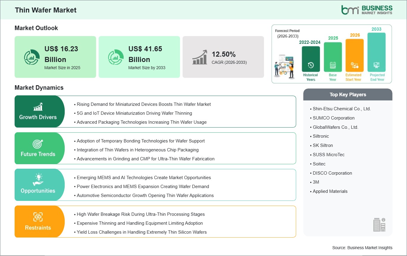
The Thin Wafer Market size is expected to reach US$ 41.65 billion by 2033 from US$ 16.23 billion in 2025. The market is estimated to record a CAGR of 12.50% from 2026 to 2033.
The Global Thin Wafer Market is witnessing revolutionary growth due to rising demands for superior quality semiconductor devices in various high-tech sectors. Thin wafers, which have a lower thickness compared to other semiconductor wafers, have become a necessity in the development of electronic devices due to their smaller sizes and increased need for better quality and power efficiency. The trend in miniaturized electronic devices in the consumer sector, high-quality imaging sensors, and IoT devices are some of the major market growth drivers in this segment. Thin wafers provide better thermal management and integration capabilities in various complex devices such as 3D structures and assemblies.
In conjunction with these market growth requirements, the use of technologies such as MEMS devices, RF devices in telecommunications systems, and high-density logic devices adds greater importance to this segment in the market. But the market is not without its difficulties. Cost-effective production and process scalability are hampered by high manufacturing complexity and yield loss risks brought on by wafer fragility. Additionally, manufacturers striving to maintain reliability throughout handling, bonding, and final assembly face constant challenges due to the strict quality and defect control requirements in ultra-thin wafer processing.
Despite these limitations, new applications are still being made possible by advancements in carrier-less Taiko processes, temporary bonding techniques, and sophisticated grinding and polishing techniques. The market is positioned to change in step with the evolving needs of end-use industries, especially as the need for improved computing capabilities is driven by autonomous technologies and artificial intelligence.

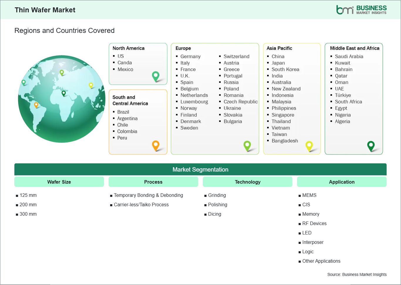
Key segments that contributed to the derivation of the thin wafer market analysis are wafer size, process, technology and application.
The proliferation of miniaturized electronic devices across the globe is one of the defining trends in the thin wafer market. As manufacturers seek to design devices that are smaller, slimmer, and more powerful, the semiconductor components need to adapt in order to accommodate these changes. Thin wafers are playing a vital role in the development of these design considerations, as they are helping reduce the size of the integrated components while allowing for the development of advanced packaging technologies.
The consumer electronics market, including devices like smartphones, wearables, wireless earbuds, etc., are now largely dependent on ultra-thin chip technology, which helps deliver superior performance in a compact size, thereby fueling the demand for wafer thinning services across the globe. Apart from consumer electronics, the industrial market is playing a vital role in the development of the thin wafer market, as these wafers are allowing manufacturers in the automation, robotics, and sensor market to design heterogeneous systems in a constrained space. For example, in the case of smart manufacturing devices, manufacturers require highly reliable MEMS sensors with superior sensitivity while offering robust structural integrity, which is achievable with the help of thin wafers.
Emerging technologies such as MEMS and artificial intelligence are unlocking new avenues for thin wafer market expansion. MEMS devices, which include accelerometers, micro‑pressure sensors, and optical switches, increasingly rely on thin wafers for enhanced sensitivity and rapid response times. Globally, industries ranging from automotive safety systems to consumer electronics and healthcare instrumentation are integrating MEMS components, reinforcing the need for wafer thinning processes that support precision and consistency at scale. Thin wafers enable MEMS manufacturers to push boundaries in performance without sacrificing device reliability. Artificial intelligence and machine learning applications have further stimulated the demand for advanced semiconductor architectures that leverage thin wafer technologies.
AI processors and neuromorphic chips require novel packaging techniques to support high‑density interconnects and multi‑die configurations. These complex designs benefit from thin wafers that minimize signal latency and improve overall system efficiency. Research and development initiatives in regions like North America and Asia Pacific are accelerating the adoption of thin wafers in AI‑oriented chips, broadening the market scope beyond traditional consumer and industrial applications to include next‑generation computing platforms.
The thin wafer market demonstrates steady growth, with size and share analysis highlighting evolving trends and competitive dynamics among key players. The report examines subsegments categorized within wafer size, process, technology and application, offering insights into their contribution to overall market performance.
By wafer size, the 300 mm subsegment dominated the market in 2025, driven by higher chip throughput and cost efficiency in advanced semiconductor production for Thin Wafer Market.
Based on process, the temporary bonding & debonding subsegment dominated the market in 2025, driven by precise handling and reduced wafer breakage during ultra-thin processing for Thin Wafer Market.
Based on technology, the grinding subsegment dominated the market in 2025, driven by achieving targeted wafer thickness and uniformity before further finishing steps for Thin Wafer Market.
Based on application, the memory subsegment dominated the market in 2025, driven by demand for high-density, miniaturized memory devices requiring enhanced integration and performance for Thin Wafer Market.
| Report Attribute | Details |
|---|---|
| Market size in 2025 | US$ 16.23 Billion |
| Market Size by 2033 | US$ 41.65 Billion |
| Global CAGR (2026 - 2033) | 12.50% |
| Historical Data | 2022-2024 |
| Forecast period | 2026-2033 |
| Segments Covered | By Wafer Size
|
|
Regions and Countries Covered
| |
| North America | US, Canada, Mexico |
| Europe | Belgium, Austria, Finland, Denmark, Greece, Poland, Romania, Russia, Ukraine, Czech Republic, Slovakia, Bulgaria, Italy, Luxembourg, Germany, Switzerland, France, Netherlands, Norway, Portugal, Spain, Sweden, United Kingdom |
| Asia-Pacific | Australia, China, India, Japan, South Korea, Indonesia, Malaysia, Philippines, Singapore, Thailand, Vietnam, Bangladesh, New Zealand, Taiwan |
| South and Central America | Brazil, Argentina, Peru, Chile, Colombia |
| Middle East and Africa | Bahrain, Kuwait, Oman, Qatar, Saudi Arabia, United Arab Emirates, Turkiye, South Africa, Egypt, Algeria, Nigeria |
| Market leaders and key company profiles |
|
The "Thin Wafer Market Size and Forecast (2022 - 2033)" report provides a detailed analysis of the market covering below areas:
The geographical scope of the Thin Wafer Market report is divided into North America, Asia Pacific, Europe, Middle East & Africa, and South & Central America. North America held the largest share in 2025.
North America is the leading region in the global Thin Wafer Market, with a strong foundation of semiconductor infrastructure, R&D facilities, and the presence of prominent wafer manufacturers. The region is served by a strong industrial base with high demand from the automotive, aerospace, defense, and medical electronic industries. These industries require precise and reliable products. The increasing trend of electric vehicles, autonomous driving technologies, and artificial intelligence-based computing platforms is boosting the demand for thin wafers in the production of miniature and highly efficient chip technology. The government is also providing incentives and making strategic investments in the semiconductor industry. This is boosting the growth of the Thin Wafer Market in the region.
The Asia Pacific region is becoming a new growth center for the Thin Wafer Market, driven by the presence of semiconductor leaders in Taiwan, South Korea, Japan, and China. The mass production of electronic devices, smartphones, and LEDs is boosting the Thin Wafer Market in the region. The region is served by strong semiconductor and wafer manufacturing facilities. This is making it easy to produce thin wafers at a low cost. The region is also seeing healthy growth in MEMS, CIS, and logic device areas, with more investments being made in advanced wafer processing technologies.
Europe's market growth is primarily driven by high-value industrial applications, especially in the areas of aerospace, automotive, and healthcare electronics. Advanced manufacturing capabilities in countries such as Germany, France, and the Netherlands are encouraging the use of advanced wafer processing technologies, especially grinding, polishing, and dicing. Manufacturers in Europe are focusing on integrating MEMS sensor and advanced packaging solutions for automotive and industrial applications.
Middle East & Africa is an emerging market for semiconductors due to increased investments in electronics manufacturing, smart infrastructure initiatives, and high-end defense and medical devices in the UAE and South Africa.
South & Central America, led by Brazil and Mexico, is gradually emerging as a market for semiconductors due to increased demand for consumer electronics, automotive sensors, and industrial devices. Although this region is not an ideal place for semiconductor fabrication plants, increased interest in advanced packaging and wafer thinning technology is an emerging growth opportunity.

The Thin Wafer Market is evaluated by gathering qualitative and quantitative data post primary and secondary research, which includes important corporate publications, association data, and databases. A few of the key developments in the thin wafer market are:
The Thin Wafer Market is valued at US$ 16.23 Billion in 2025, it is projected to reach US$ 41.65 Billion by 2033.
As per our report Thin Wafer Market, the market size is valued at US$ 16.23 Billion in 2025, projecting it to reach US$ 41.65 Billion by 2033. This translates to a CAGR of approximately 12.50% during the forecast period.
The Thin Wafer Market report typically cover these key segments-
The historic period, base year, and forecast period can vary slightly depending on the specific market research report. However, for the Thin Wafer Market report:
The Thin Wafer Market is populated by several key players, each contributing to its growth and innovation. Some of the major players include:
The Thin Wafer Market report is valuable for diverse stakeholders, including:
Essentially, anyone involved in or considering involvement in the Thin Wafer Market value chain can benefit from the information contained in a comprehensive market report.
Please tell us your area of interest
(Market Segments/ Regions and Countries/ Companies)