
Semiconductor Assembly And Packaging Equipment Market Outlook: Size, Share, Trends, Growth Analysis, Competitive Landscape & Forecast, 2026-2033

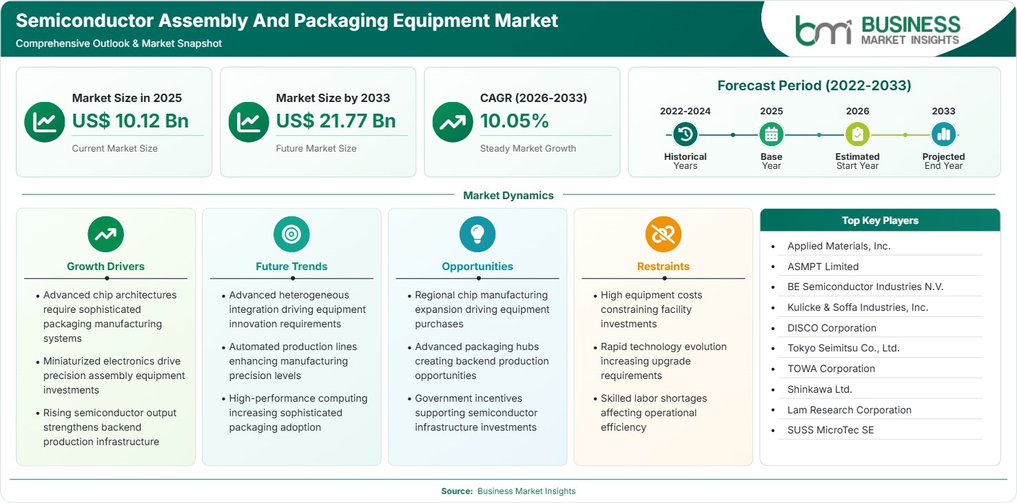
The Semiconductor Assembly and Packaging Equipment Market size was valued at US$ 10.12 billion in 2025 and is projected to reach US$ 21.77 billion by 2033, growing at a CAGR of 10.05% during 2026–2033, driven by advanced packaging, AI computing, HBM, chiplets, automotive electrification, OSAT expansion, and semiconductor localization investments.

Report Coverage
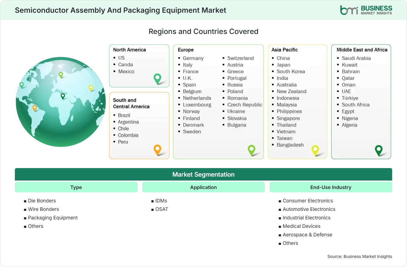
  • Type: Die Bonders, Wire Bonders, Packaging Equipment, Others
  • Application: IDMs, OSAT
  • End-Use Industry: Consumer Electronics, Automotive Electronics, Industrial Electronics, Medical Devices, Aerospace & Defense, Others
US$ 10.12 Bn Market size in 2025
US$ 21.77 Bn Market Size by 2033
10.05% CAGR, 2026 - 2033
2026-2033 Forecast Period

AI Overview

Semiconductor Assembly And Packaging Equipment Market Summary

  • North America Region: North America holds a 18%–21% share in 2025, growing with a 9.0%–10.0% CAGR during 2026–2033, influenced by domestic semiconductor investment, advanced packaging programs, AI infrastructure, reshoring, and demand for high-density integration. US demand is supported by advanced packaging investment and is projected to grow at an 8.8%–9.8% CAGR through 2033.
  • Fastest Growing Region: Asia Pacific holds a 55%–60% share in 2025, growing with a 10.5%–11.4% CAGR during 2026–2033, supported by dense semiconductor ecosystems, OSAT expansion, advanced packaging adoption, electronics exports, AI hardware demand, and sustained capacity investment.
  • Leading Segment: Wire Bonders hold a 28%–32% share in 2025, growing with a 9.2%–10.0% CAGR during 2026–2033, supported by mature high-volume assembly, automotive electronics, power devices, copper-wire adoption, automation, and throughput optimization.
  • High Growth Segment: Packaging Equipment holds a 24%–28% share in 2025, growing with an 11.2%–12.0% CAGR during 2026–2033, supported by fan-out, wafer-level packaging, advanced substrates, molding, HBM, chiplets, and increasing OSAT investment.
  • Key Market Opportunity: Integrated equipment platforms combining bonding, molding, process control, automation, software, and analytics can capture demand for higher yields, faster qualification, flexible architectures, and localized production.
  • Major Market Players: Applied Materials, Inc.; ASMPT Limited; BE Semiconductor Industries N.V.; Kulicke & Soffa Industries, Inc.; DISCO Corporation; Tokyo Seimitsu Co., Ltd.; TOWA Corporation; Shinkawa Ltd.; Lam Research Corporation; SUSS MicroTec SE.
Strategic Insights

Semiconductor Assembly And Packaging Equipment Market: Strategic Insights

Semiconductor Assembly And Packaging Equipment Market Strategic Framework
FREE PDF
Request your free sample
Request free sample
Stakeholder View

Key Takeaways

  • The chain of value is growing more integrated, with equipment suppliers working closely with IDMs, OSATs, substrate manufacturers, materials companies, and chip designers. Nowadays, the choice of equipment is based more on process capability, software integration, uptime, service coverage, and package compatibility than on the individual economics of the machine.
  • Advanced packaging provides the greatest potential for incremental growth since AI accelerators, HBM, chiplets, and heterogeneous integration demand a higher level of precision than is required by traditional assembly methods. More investment attention should therefore be given to advanced die bonding, packaging systems, metrology, and process-control platforms.
  • There is a trend towards the use of closed-loop manufacturing in terms of equipment innovation, since features such as machine vision, predictive maintenance, real-time monitoring, automated recipe control, and analytics have become important to avoid substantial increases in manufacturing costs resulting from yield losses in complex multi-die assemblies.
  • The Asia Pacific region has the most compelling case for investment since it brings together a large amount of existing semiconductor capacity with a dense network of OSAT infrastructure. The countries of Taiwan, South Korea, China, Japan, and Singapore each have strong points in the areas of memory, foundry, assembly, materials, and equipment.
  • More of your investment is now being directed towards technology partnerships and expanding your portfolio. In 2026, Applied Materials entered an agreement to acquire ASMPT's NEXX business, which extended its range of panel-level advanced packaging and shows the strategic value of larger-format packaging technologies.
  • Qualification credibility is still a major obstacle in terms of competition. Semiconductor manufacturers place importance on process stability, uptime, application engineering, yield performance, and compatibility with developing package architectures, which in turn enhances the significance of installed bases and customer co-development.
Geographic Outlook

Semiconductor Assembly And Packaging Equipment Market Regional Highlights

North America Semiconductor Assembly And Packaging Equipment Market

North America holds an 18%–21% share in 2025 and is projected to grow at a 9.0%–10.0% CAGR during 2026–2033. Semiconductor Assembly And Packaging Equipment Market share is supported by US semiconductor investment, advanced packaging research, AI infrastructure, and supply-chain resilience initiatives. Demand is strongest across AI, automotive, defense, and high-performance computing.

  • The strengthening of investment in US semiconductors is leading to greater demand for bonding, packaging, inspection, and process-control systems since manufacturers are expanding their domestic backend capabilities and aiming to establish shorter, more resilient supply chains.
  • The demand for advanced bonding, HBM integration, thermal management, alignment accuracy, and yield monitoring in the production of AI accelerators is growing as semiconductor packages become more complex.
  • The strategies for reshoring help promote market growth by stimulating the production of key semiconductor components within the country and decreasing reliance on the existing concentrated backend manufacturing networks.
  • Mexico offers supplementary capacity for the manufacture of electronics, while Canada fosters specialized ecosystems for semiconductors and photonics, thus providing special opportunities for suppliers who can provide regional technical support and flexible equipment platforms.

US Semiconductor Assembly And Packaging Equipment Market

The US represents approximately 78%–82% of the North American Semiconductor Assembly and Packaging Equipment Market demand in 2025 and is projected to grow at an 8.8%–9.8% CAGR during 2026–2033. Domestic semiconductor incentives, advanced packaging research, AI infrastructure, and defense requirements support demand. The country combines technology developers, equipment suppliers, IDMs, fabless chip companies, and research institutions.

  • There is growing demand for systems that support chiplets, HBM, 2.5D integration, hybrid bonding, and high-density interconnect architectures because of advanced packaging programs.
  • The need for local service, application engineering, qualification support, spare parts, and lifecycle management is increasing due to the expansion of semiconductor production at home.
  • The demand for bonding, deposition, metrology, molding, inspection, and process-control technologies needed to support high-performance packages is increasing due to advances in AI infrastructure.

Europe Semiconductor Assembly And Packaging Equipment Market

Europe holds a 13%–16% share in 2025 and is projected to grow at an 8.2%–9.2% CAGR during 2026–2033. Germany leads regional demand, supported by automotive and industrial semiconductor applications. Germany is projected at an 8.5%–9.5% CAGR, while the Netherlands is positioned at approximately 9.0%–10.0% CAGR. Semiconductor Assembly and Packaging Equipment Market growth is linked to automotive electronics, power semiconductors, industrial automation, and supply-chain localization.

  • The automotive and industrial sector in Germany is able to provide reliable packaging equipment, as well as assembly of power devices, automation, and the capability to meet high-throughput production requirements.
  • The Netherlands has both expertise in semiconductor equipment and research abilities, which enable it to carry out precise assembly, wafer processing, and the development of advanced packaging.
  • France and Italy offer opportunities associated with applications in the automotive, aerospace, defense, and industrial semiconductor sectors, thereby promoting selective backend localization.
  • Ireland continues to be relevant since its existing base in semiconductor manufacturing provides support for process equipment, automation, and advanced production infrastructure.

Asia Pacific Semiconductor Assembly And Packaging Equipment Market

Asia Pacific holds a 55%–60% share in 2025 and is projected to grow at a 10.5%–11.4% CAGR during 2026–2033. Semiconductor Assembly and Packaging Equipment Market share is supported by concentrated OSATs, foundries, IDMs, memory manufacturers, and electronics producers. Taiwan, South Korea, China, and Japan remain core demand centers. Taiwan is projected at 10.8%–11.7% CAGR, while India offers a higher-growth opportunity at 11.5%–12.5% CAGR as backend capacity develops.

  • Taiwan is still at the heart of the demand for advanced packaging since the top manufacturers need sophisticated bonding, wafer-level packaging, metrology, and process-control systems for use in high-performance computing.
  • The demand for precision bonding, thermal processing, inspection, and advanced packaging equipment is supported by South Korea's investments in memory and HBM.
  • China is still increasing its domestic semiconductor capacity, which is generating equipment opportunities as a result of export controls and localization policies altering procurement strategies.
  • By combining its expertise in semiconductor equipment with the demand from the automotive and industrial sectors, Japan is supporting investment in high-reliability assembly and packaging.
  • India is putting in place its backend infrastructure and thus provides long-term opportunities for suppliers who set up local services, training, and application-engineering capabilities.

Rest of World Semiconductor Assembly And Packaging Equipment Market

South and Central America represent a smaller but developing opportunity supported by electronics, automotive, and industrial manufacturing. Brazil and Mexico provide the strongest prospects. The Middle East and Africa demand is concentrated in specialized electronics, defense, industrial systems, and emerging technology initiatives. Semiconductor Assembly And Packaging Equipment Market share across the Rest of World is estimated at 7%–10% in 2025, with an 8.0%–9.0% CAGR during 2026–2033. Brazil and Mexico provide the strongest Latin American opportunities, while Israel and the Gulf states offer specialized technology prospects.

  • As Brazil's electronics, automotive, and industrial sectors develop, opportunities for local semiconductor assembly and the provision of equipment services within the growing manufacturing ecosystems arise.
  • Mexico has the advantage of being close to the electronics and semiconductor supply chains of the US, which enables business opportunities related to manufacturing diversification and nearshoring.
  • Israel has a demand for specialized semiconductors and those related to defense, which is backed by the development of advanced electronics and the production of high-value technologies.
  • The economies of the Gulf are putting their money into technology infrastructure and industrial diversification, which is leading to a selection of opportunities in the field of semiconductor-related manufacturing and engineering services.
  • In South Africa, there are fewer opportunities available in the fields of specialized electronics, industrial systems, research, and semiconductor activities linked to technology.
Global Market Geography
FREE PDF
Request your free sample
Request free sample
Segment Analysis

Semiconductor Assembly And Packaging Equipment Market Segmentation

Type

Type represents a core equipment hierarchy spanning established interconnection tools and advanced packaging systems. Wire Bonders hold a 28%–32% Semiconductor Assembly and Packaging Equipment Market share in 2025 with a 9.2%–10.0% CAGR during 2026–2033. Packaging Equipment holds 24%–28% with an 11.2%–12.0% CAGR, reflecting faster advanced-package adoption.

  • Die Bonders: Precision die placement supports multi-die assemblies, power semiconductors, sensors, and advanced packages, with automation and alignment accuracy improving productivity and heterogeneous integration.
  • Wire Bonders: Mature high-volume interconnection remains essential across consumer, automotive, industrial, and power devices, while copper-wire adoption, automation, finer pitches, and throughput improvements sustain demand.
  • Packaging Equipment: Molding, encapsulation, plating, and related systems support package protection and advanced formats, while OSAT expansion increases flexibility and process-control requirements.

Application

IDMs hold a 54%–58% Semiconductor Assembly and Packaging Equipment Market share in 2025 and a 9.3%–10.1% CAGR during 2026–2033, supported by integrated manufacturing and advanced packaging investments. OSAT demand is expanding faster at a 10.6%–11.5% CAGR, reflecting outsourced assembly growth and geographic capacity diversification.

  • IDMs: Integrated manufacturers prioritize process control, product differentiation, advanced packaging, and high-volume production while retaining direct control over qualification and manufacturing integration.
  • OSAT: Outsourced assembly providers require flexible, scalable equipment supporting multiple customers, package types, and production volumes while improving utilization and reducing qualification time.

End-Use Industry

Consumer Electronics represents the largest end-use category at an estimated 27%–31% share in 2025, while the end-use category expands at approximately 9.4%–10.4% CAGR through 2033. Automotive, aerospace, and industrial applications are gaining strategic importance as electrification, sensing, reliability, and computing requirements increase packaging complexity.

  • Consumer Electronics: Smartphones, wearables, computers, and connected products require compact packages, high throughput, and cost-efficient assembly, sustaining demand for mature and advanced packaging systems.
  • Automotive Electronics: Electrification, ADAS, power electronics, and vehicle computing require highly reliable packages with stringent thermal, mechanical, and lifecycle requirements.
  • Industrial Electronics: Automation, robotics, power management, and control systems support demand for durable packages, sensors, power semiconductors, and reliable high-volume assembly.
  • Medical Devices: Imaging, monitoring, diagnostics, and portable devices require compact semiconductor packages, while traceability and reliability support specialized equipment requirements.
  • Aerospace and Defense: High-reliability electronics require controlled manufacturing, repeatable precision, stringent quality processes, and advanced inspection capabilities.
Market Forces

Semiconductor Assembly And Packaging Equipment Market Dynamics

Key Market Drivers

Advanced Packaging Raises Equipment Intensity

Advanced packaging is increasing equipment intensity because chiplets, HBM, 2.5D integration, and 3D structures require tighter alignment, bonding, deposition, molding, inspection, and thermal control. Semiconductor Assembly and Packaging Equipment Market growth is increasingly linked to package complexity rather than semiconductor unit shipments alone. Packaging equipment benefits from fan-out, wafer-level, hybrid-bonding, and heterogeneous-integration adoption. Applied Materials introduced new CMP, deposition, and eBeam metrology systems in June 2026 for advanced packaging and HBM applications, demonstrating the industry's movement toward integrated process control.

OSAT Expansion Increases Equipment Procurement

OSAT providers are expanding capacity as fabless semiconductor companies outsource more assembly and test activities. This creates recurring demand for bonding, molding, packaging, automation, and process-control equipment. OSATs must support multiple customers and package architectures, making flexible configurations and rapid qualification increasingly important. Capacity development in Asia Pacific is especially influential because the region combines major OSATs with fabs, substrates, materials suppliers, and engineering ecosystems. The resulting Semiconductor Assembly and Packaging Equipment Market trends are increasingly shaped by OSAT utilization, new facility construction, advanced-package adoption, and equipment replacement cycles.

AI And HBM Raise Precision Requirements

AI accelerators require greater bandwidth and energy efficiency, encouraging multi-die integration and HBM architectures that increase demands on backend manufacturing. HBM introduces challenges involving thin dies, warpage, thermal management, bonding accuracy, and defect control. Applied Materials' June 2026 product introduction included systems targeting HBM stacking and advanced packaging metrology. These developments reinforce the Semiconductor Assembly and Packaging Equipment Market growth toward tools combining precision, process monitoring, automation, and yield management.

Key Market Opportunities

Hybrid Bonding Creates Premium Equipment Demand

Hybrid bonding creates opportunities across bonding equipment, alignment, cleaning, surface preparation, metrology, and process control. The technology enables dense interconnects for advanced memory and logic architectures and therefore increases equipment value per package. BE Semiconductor Industries reported Q2 2026 revenue of €249.9 million, up 68.7% year over year, with orders up 128.8%, citing strong demand including hybrid bonding, photonics, and data-center applications. Semiconductor Assembly and Packaging Equipment Market Forecasts should therefore recognize hybrid bonding as a premium technology pathway with increasing qualification activity.

Panel-Level Packaging Expands Addressable Markets

Panel-level packaging creates opportunities across deposition, plating, lithography, inspection, handling, and process control as AI packages increase in physical size. Applied Materials announced in May 2026 an agreement to acquire ASMPT's NEXX business, strengthening its panel-level advanced packaging portfolio. The transaction targets larger-body AI accelerators and packaging formats extending beyond conventional wafer dimensions. The Semiconductor Assembly and Packaging Equipment Market opportunity, therefore, extends into large-area manufacturing, where process uniformity and equipment scalability become important competitive factors.

Localized Backend Capacity Creates New Demand

Governments and semiconductor manufacturers are developing geographically diversified backend capacity to strengthen supply-chain resilience. This creates opportunities for suppliers that establish local application laboratories, technical teams, training, and process-development partnerships. India, the US, and Europe are developing capabilities that can broaden the geographic footprint of advanced packaging. Equipment vendors can improve market access through modular platforms supporting multiple package types and qualification requirements. The Semiconductor Assembly and Packaging Equipment Market scope is consequently expanding beyond established Asian production centers toward emerging regional manufacturing clusters.

Market Restraints and Challenges

Export Controls Increase Supply-Chain Complexity

Export controls, trade restrictions, localization requirements, and evolving rules governing access to technology in major manufacturing countries affect semiconductor equipment supply chains. As a result, suppliers may have to go through longer qualification periods, deal with fragmented product configurations, incur extra compliance costs, and face uncertainty concerning their customers' procurement schedules. Advanced packaging equipment is becoming more strategic since it supports applications in the fields of artificial intelligence, memory, automotive systems, and defense, which in turn leads to greater regulatory oversight.

Qualification Complexity Raises Development Costs

Factor: Advanced packaging requires coordinated control of equipment, materials, substrates, process recipes, thermal conditions, metrology, and semiconductor designs. Impact: equipment suppliers can face higher R&D costs, longer commercialization periods, and extended customer qualification cycles. HBM and multi-die packages are particularly demanding because defects can compromise expensive assemblies containing multiple integrated components. Customers generally require extensive process validation before approving equipment for volume production.

Company Analysis

Competitive Landscape

The Semiconductor Assembly and Packaging Equipment Market analysis indicates that competition is shifting from standalone machine performance toward integrated process capability, advanced packaging expertise, service coverage, automation, and customer co-development.

Company Name

Overview

Products and Services relevant to this market

Applied Materials, Inc.

Global semiconductor equipment supplier expanding advanced packaging, bonding, metrology, deposition, and process-control capabilities.

Advanced packaging deposition, CMP, plating, eBeam metrology, inspection, process control, and packaging technologies.

ASMPT Limited

Major assembly equipment provider with broad die, wire, placement, and advanced packaging capabilities.

Die bonding, wire bonding, thermocompression bonding, advanced packaging, automation, and process solutions.

BE Semiconductor Industries N.V.

Specialist assembly equipment manufacturer with strong die attach and advanced bonding capabilities.

Die attach, hybrid bonding, thermocompression bonding, packaging automation, and semiconductor assembly systems.

Kulicke & Soffa Industries, Inc.

Established semiconductor assembly supplier with significant wire bonding and packaging expertise.

Wire bonders, die bonders, wedge bonding, advanced packaging, and semiconductor assembly systems.

DISCO Corporation

Japanese precision equipment manufacturer serving semiconductor cutting, grinding, and wafer processing.

Dicing systems, grinders, cutting tools, wafer processing equipment, and production support technologies.

Tokyo Seimitsu Co., Ltd.

Semiconductor equipment provider serving wafer processing, metrology, probing, and precision manufacturing.

Dicing, wafer probing, metrology, inspection, grinding, and semiconductor manufacturing equipment.

TOWA Corporation

Japanese packaging equipment specialist with strong molding and encapsulation capabilities.

Compression molding, transfer molding, packaging equipment, molds, and semiconductor production solutions.

Shinkawa Ltd.

Semiconductor assembly technology provider focused on bonding, packaging, and precision manufacturing.

Wire bonding, die bonding, semiconductor assembly equipment, and automated packaging solutions.

Lam Research Corporation

Major semiconductor equipment company with technologies supporting advanced process integration and packaging.

Deposition, etch, clean, advanced packaging process technologies, and integrated manufacturing solutions.

SUSS MicroTec SE

Specialist equipment company serving advanced packaging, wafer bonding, lithography, and semiconductor applications.

Wafer bonding, lithography, coating, cleaning, hybrid bonding support, and advanced packaging equipment.

Trust & Transparency

Research Methodology

The market analysis combines proprietary research with secondary data from government agencies, company disclosures, regulatory filings, industry databases and expert interviews. Market estimates are validated through data triangulation, cross-market benchmarking and analyst review.

View Full Research Methodology

Questions Answered

Frequently Asked Questions

Which applications offer the strongest long-term equipment opportunity?

AI computing, HBM, automotive electronics, advanced mobile processors, power semiconductors, and industrial automation offer strong opportunities. These applications combine increasing semiconductor content with demanding requirements for bandwidth, thermal performance, reliability, miniaturization, and heterogeneous integration.

What role does metrology play in advanced packaging?

Metrology helps control alignment, thickness, dimensional accuracy, warpage, and defects as package architectures become more complex. Its integration with manufacturing equipment improves process visibility and supports earlier identification of conditions that could reduce yield in high-value multi-die assemblies.

How are OSAT companies influencing equipment demand?

OSAT expansion increases demand for flexible, high-throughput equipment because outsourced manufacturers must support multiple customers and package designs. Their investment cycles depend on customer qualifications, utilization rates, advanced packaging adoption, and geographic capacity expansion.

Why does wire bonding remain important despite advanced packaging adoption?

Wire bonding remains widely used because it is mature, scalable, cost-efficient, and compatible with consumer, automotive, industrial, and power packages. Copper-wire adoption, automation, finer pitches, and higher throughput continue improving its competitiveness, where extreme interconnect density is unnecessary.

What does the Semiconductor Assembly and Packaging Equipment Market Report cover?

The Semiconductor Assembly And Packaging Equipment Market Report covers market size, growth outlook, regional trends, equipment types, applications, end-use industries, competitive developments, key drivers, opportunities, restraints, and emerging technologies shaping semiconductor assembly and packaging equipment demand through 2033.

Access the Full Semiconductor Assembly And Packaging Equipment Market Report

Get segment-level forecasts, regional estimates, competitive benchmarking, company profiles and downloadable Excel datasets.

Access the full Semiconductor Assembly And Packaging Equipment Market Report
350 pages PDF & Excel | 2026-10-12
Similar Research

Related Market Reports