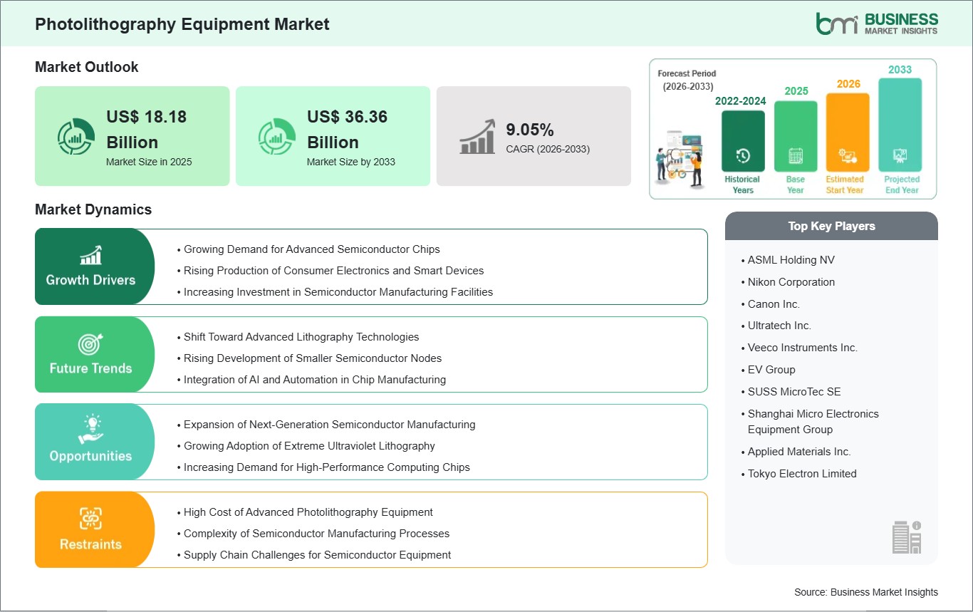
The Photolithography Equipment Market size is expected to reach US$ 36.36 billion by 2033 from US$ 18.18 billion in 2025. The market is estimated to record a CAGR of 9.05% from 2026 to 2033.
Executive Summary and Global Market Analysis:
The market for photolithography equipment is growing due to the development of advanced chips by semiconductor manufacturers for modern electronic applications. Photolithography is an important technology used in semiconductor manufacturing to transfer circuit patterns onto silicon wafers. This technology helps in the fabrication of integrated circuits for smartphones, computers, automotive electronics, communication devices, and industrial equipment. With the growing demand for smaller, faster, and more efficient semiconductor chips, manufacturers are using advanced lithography equipment for precise circuit designs and enhanced chip performance.
The increasing demand for digital technology like artificial intelligence, high-performance computing, and communication systems is fueling the need for advanced semiconductor manufacturing. The semiconductor industry is investing in new fabrication facilities and enhancing existing ones to support the development of next-generation semiconductors. Photolithography systems are critical in facilitating these manufacturing operations by enabling accurate and reliable chip patterning. With the increasing reliance of various industries on semiconductor technology, the demand for advanced photolithography systems is expected to increase steadily in the semiconductor manufacturing industry.
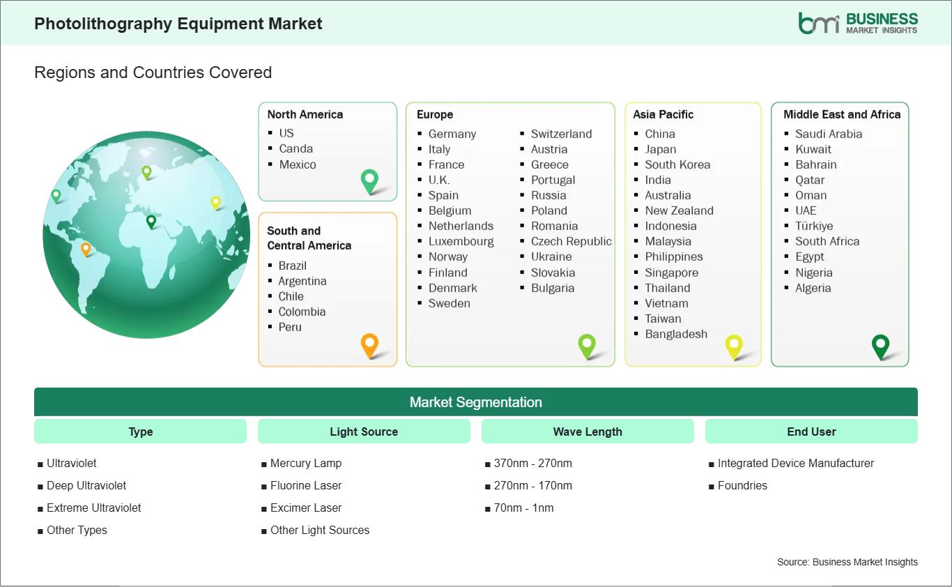
Key segments that contributed to the derivation of the photolithography equipment market analysis are type, light source, wave length, end user.
By type, the photolithography equipment market is segmented into ultraviolet, deep ultraviolet, extreme ultraviolet, and others. The deep ultraviolet segment dominated the market in 2025.
By light source, the market is classified into mercury lamp, fluorine laser, excimer laser, and others. The excimer laser segment dominated the market in 2025.
By wave length, the market is segmented into 370nm - 270nm, 270nm - 170nm, and 70nm - 1nm. The 270nm - 170nm segment dominated the market in 2025.
By end user, the market is segmented into integrated device manufacturer and foundries. The foundries segment dominated the market in 2025.
Photolithography Equipment Market Drivers and Opportunities:
Growing Demand for Advanced Semiconductor Chips
The increasing demand for modern semiconductor chips is pushing up the markets for photolithography equipment since semiconductor devices are found in a variety of products. Smart phones, computers, automotive electronics, communications equipment and other consumer products all contain semiconductor chips. As technology continues to grow, the need for smaller, faster and more power-efficient semiconductor chips will also continue to grow. Photolithography equipment is essential for creating accurate circuit patterns on semiconductor wafers, therefore enabling manufacturers to produce the latest integrated circuits.
Electronics manufacturers are continuously developing new products that require high-performance chips. Applications such as artificial intelligence systems, data centers, electric vehicles, and advanced communication technologies rely on powerful semiconductor components. To produce these chips, semiconductor fabrication facilities require advanced photolithography systems capable of achieving higher precision and smaller circuit patterns.
In addition, increasing global demand for digital devices is encouraging semiconductor companies to expand manufacturing capacity. New fabrication plants and upgrades to existing facilities require advanced lithography equipment for chip production. As industries continue to depend on powerful and efficient semiconductor technologies, the demand for photolithography equipment is expected to grow across the global semiconductor manufacturing ecosystem.
Expansion of Next-Generation Semiconductor Manufacturing
The expansion of next-generation semiconductor manufacturing presents strong opportunities for the photolithography equipment market. Semiconductor manufacturers are investing in advanced fabrication technologies to produce smaller and more efficient chips for modern electronic applications. These new manufacturing processes require highly precise lithography systems that can create extremely small circuit patterns on semiconductor wafers.
Next-generation semiconductor technologies are essential for applications such as artificial intelligence, advanced computing, high-speed communication networks, and autonomous vehicles. These applications require powerful chips with higher processing capability and improved energy efficiency. Photolithography equipment plays a central role in enabling the production of these advanced semiconductor devices.
Many semiconductor companies and governments are investing in new fabrication facilities to strengthen chip manufacturing capacity. These investments support the adoption of advanced lithography technologies that enable higher precision and improved production capabilities. As semiconductor manufacturers continue to develop next-generation chips and expand fabrication capacity, the demand for advanced photolithography equipment is expected to grow significantly in the coming years.
Photolithography Equipment Market Size and Share Analysis:
The global photolithography equipment market is experiencing steady growth, with market size and share analysis reflecting evolving treatment preferences and competitive dynamics among key players. The report evaluates important subsegments categorized within type, light source, wave length, end user, highlighting their respective contributions to overall market performance.
By type, the deep ultraviolet subsegment dominated the market in 2025, due to its wide use in semiconductor manufacturing for producing high-resolution circuit patterns required for advanced and high-performance electronic chips.
By light source, the excimer laser subsegment dominated the market in 2025, because it enables precise and stable light generation required for advanced photolithography processes used in semiconductor fabrication and microelectronics manufacturing.
By wave length, the 270nm - 170nm subsegment dominated the market in 2025, as this wavelength range is widely used in deep ultraviolet lithography systems for producing fine semiconductor patterns with high precision.
By end user, the foundries subsegment dominated the market in 2025, due to the growing demand for semiconductor fabrication services from electronics companies that outsource chip manufacturing to specialized foundry facilities.
Australia, China, India, Japan, South Korea, Indonesia, Malaysia, Philippines, Singapore, Thailand, Vietnam, Bangladesh, New Zealand, Taiwan
South and Central America
Brazil, Argentina, Peru, Chile, Colombia
Middle East and Africa
Bahrain, Kuwait, Oman, Qatar, Saudi Arabia, United Arab Emirates, Turkiye, South Africa, Egypt, Algeria, Nigeria
Market leaders and key company profiles
ASML Holding NV
Nikon Corporation
Canon Inc.
Ultratech Inc.
Veeco Instruments Inc.
EV Group
SUSS MicroTec SE
Shanghai Micro Electronics Equipment Group
Applied Materials Inc.
Tokyo Electron Limited
Get more information on this report
Photolithography Equipment Market Report Coverage and Deliverables:
The "Photolithography Equipment Market Size and Forecast (2022 - 2033)" report provides a detailed analysis of the market covering below areas:
Photolithography Equipment market size and forecast at the regional and country levels for segments covered under the scope
Photolithography Equipment market trends, as well as drivers, restraints, and opportunities
Photolithography Equipment market analysis covering key trends, regional framework, major players, regulations, and recent developments
Industry landscape and competition analysis covering market concentration, heat map analysis, prominent players, and recent developments for the Photolithography Equipment market
Detailed company profiles, including SWOT analysis
The geographical scope of the photolithography equipment market report is divided into: North America, Asia Pacific, Europe, Middle East & Africa, and South & Central America. North America held the largest share in 2025.
North America dominates the photolithography equipment market due to strong semiconductor research, advanced technology development, and the presence of leading semiconductor companies. The region has a well-established semiconductor ecosystem that includes chip designers, manufacturing equipment suppliers, and technology research institutions. These factors support continuous innovation in semiconductor manufacturing technologies, including advanced lithography systems used in chip fabrication.
Semiconductor manufacturers in North America are investing in advanced production technologies to support the development of high-performance chips for applications such as artificial intelligence, cloud computing, and advanced communication systems. The region also benefits from strong collaboration between technology companies, research organizations, and semiconductor equipment manufacturers. These collaborations encourage the development of innovative manufacturing solutions that improve chip performance and production efficiency.
In addition, governments and private companies in North America are supporting semiconductor manufacturing through investments in research and infrastructure. These initiatives aim to strengthen regional semiconductor supply chains and encourage the adoption of advanced manufacturing technologies. As a result, North America continues to play a leading role in the development and adoption of photolithography equipment in the global semiconductor industry.
Get more information on this report
Photolithography Equipment Market Research Report Guidance:
The report includes qualitative and quantitative data in the Photolithography Equipment market across type, light source, wave length, end user, and geography.
The report starts with the key takeaways (chapter 2), highlighting the key trends and outlook of the Photolithography Equipment market.
Chapter 3 focuses on the research methodology of the study.
Chapter 4 includes ecosystem analysis.
Chapter 5 highlights the major industry dynamics in the Photolithography Equipment market, including factors that are driving the market, prevailing deterrents, potential opportunities, as well as future trends. Impact analysis of these drivers and restraints is also covered in this section.
Chapter 6 discusses the Photolithography Equipment market scenario, in terms of historical market revenues, and forecast till the year 2033.
Chapters 7 to 11 cover the Photolithography Equipment market segments by type, light source, wave length, end user, and geography across North America, Europe, Asia Pacific, the Middle East and Africa, and South and Central America. They cover the market revenue, forecast, and factors driving the market.
Chapter 12 describes the competitive analysis along with the heat map analysis for the key players operating in the market.
Chapter 13 describes the industry landscape analysis. It provides detailed descriptions of business activities such as market initiatives, new developments, mergers, and joint ventures globally, along with a competitive landscape.
Chapter 14 provides detailed profiles of the major companies operating in the Photolithography Equipment market. Companies have been profiled on the basis of their key facts, business descriptions, products, financial overview, SWOT analysis, and key developments.
Chapter 15, i.e., the appendix, is inclusive of a brief overview of the company, list of abbreviations, and disclaimer.
Photolithography Equipment Market News and Key Development:
The photolithography equipment market is evaluated by gathering qualitative and quantitative data post primary and secondary research, which includes important corporate publications, association data, and databases. A few of the key developments in the Photolithography Equipment market are:
In June 2024, ASML Holding N.V. announced that it opened a joint High-NA EUV lithography laboratory with imec in Veldhoven, the Netherlands, providing semiconductor manufacturers early access to the prototype TWINSCAN EXE:5000 High-NA EUV scanner to accelerate development and prepare the technology for high-volume manufacturing.
In October 2024, Nikon Corporation announced that it is developing a digital lithography system with 1.0-micron resolution designed for advanced semiconductor packaging applications, with plans to commercialize the system in its fiscal year 2026.
Key Sources Referred:
International Electrotechnical CommissionInstitute of Electrical and Electronics EngineersInternational Organization for StandardizationBureau of Indian StandardsCentral Electricity AuthorityMinistry of PowerIndian Electrical and Electronics Manufacturers' AssociationEuropean Committee for Electrotechnical StandardizationVDE Association for Electrical Electronic & Information TechnologiesCompany WebsitesCompany Annual ReportsCompany Investor Presentations
The List of Companies - Photolithography Equipment Market
ASML Holding NV
Nikon Corporation
Canon Inc.
Ultratech Inc.
Veeco Instruments Inc.
EV Group
SUSS MicroTec SE
Shanghai Micro Electronics Equipment Group
Applied Materials Inc.
Tokyo Electron Limited
About Author— Electronics and Semiconductor Research Team
Siddhika is an experienced market research professional with over five years of expertise in delivering actionable market intelligence and strategic insights to support business growth and decision-making. She has strong experience in designing and managing end-to-end research engagements, including research planning, data collection, and insight generation.
Proficient in research methodologies, Siddhika synthesizes diverse information sources to deliver accurate, high-quality insights and strategic recommendations. She excels at translating complex market information into strategic narratives that support executive decision-making..
Show More
Frequently Asked Questions
How big is the Photolithography Equipment Market?
The Photolithography Equipment Market is valued at US$ 18.18 Billion in 2025, it is projected to reach US$ 36.36 Billion by 2033.
What is the CAGR for Photolithography Equipment Market by (2026 - 2033)?
As per our report Photolithography Equipment Market, the market size is valued at US$ 18.18 Billion in 2025, projecting it to reach US$ 36.36 Billion by 2033. This translates to a CAGR of approximately 9.05% during the forecast period.
What segments are covered in this report?
The Photolithography Equipment Market report typically cover these key segments-
Type (Ultraviolet, Deep Ultraviolet, Extreme Ultraviolet, Other Types)
End User (Integrated Device Manufacturer, Foundries)
What is the historic period, base year, and forecast period taken for Photolithography Equipment Market?
The historic period, base year, and forecast period can vary slightly depending on the specific market research report. However, for the Photolithography Equipment Market report:
Historic Period : 2022-2024
Base Year : 2025
Forecast Period : 2026-2033
Who are the major players in Photolithography Equipment Market?
The Photolithography Equipment Market is populated by several key players, each contributing to its growth and innovation. Some of the major players include:
ASML Holding NV
Nikon Corporation
Canon Inc.
Ultratech Inc.
Veeco Instruments Inc.
EV Group
SUSS MicroTec SE
Shanghai Micro Electronics Equipment Group
Applied Materials Inc.
Tokyo Electron Limited
Who should buy this report?
The Photolithography Equipment Market report is valuable for diverse stakeholders, including:
Investors: Provides insights for investment decisions pertaining to market growth, companies, or industry insights. Helps assess market attractiveness and potential returns.
Industry Players: Offers competitive intelligence, market sizing, and trend analysis to inform strategic planning, product development, and sales strategies.
Suppliers and Manufacturers: Helps understand market demand for components, materials, and services related to concerned industry.
Researchers and Consultants: Provides data and analysis for academic research, consulting projects, and market studies.
Financial Institutions: Helps assess risks and opportunities associated with financing or investing in the concerned market.
Essentially, anyone involved in or considering involvement in the Photolithography Equipment Market value chain can benefit from the information contained in a comprehensive market report.


 Get Free Sample For Photolithography Equipment Market


