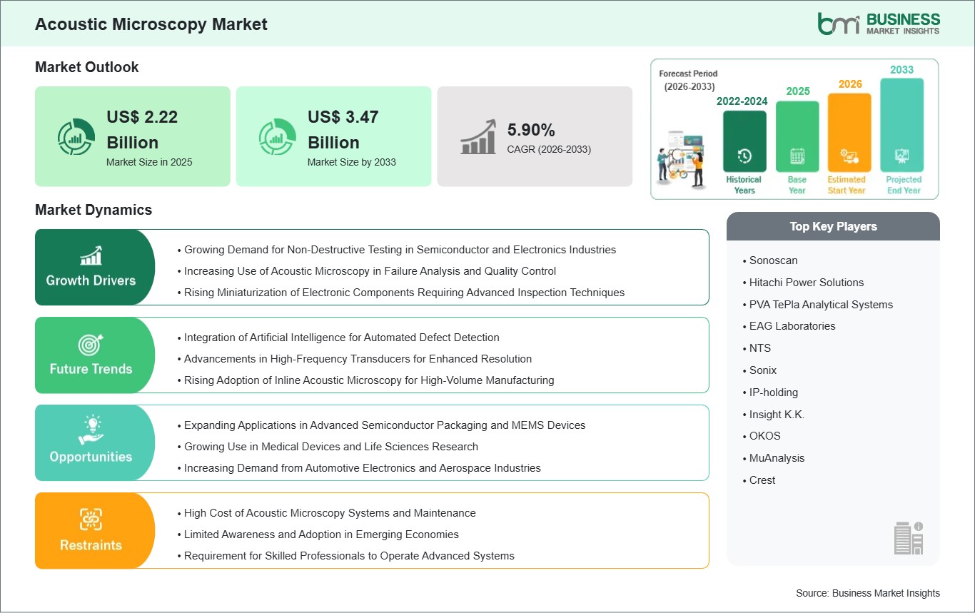
Rising Demand for Non-Destructive Testing in Advanced Industries
The growing emphasis on product reliability and safety across semiconductors, life science, material science, and nanotechnology industries is a major driver for the acoustic microscopy market. Non-destructive testing (NDT) is critical in these sectors because even minor defects or structural inconsistencies can lead to product failure, costly recalls, or safety hazards. Acoustic microscopy enables precise, high-resolution imaging of internal structures without damaging the components, making it an indispensable tool for failure analysis, quality control, and reliability testing. Its ability to detect voids, and other microstructural anomalies ensures that products meet stringent quality standards before reaching the market.
The adoption of acoustic microscopy in semiconductor fabrication is particularly noteworthy. As semiconductor devices continue to shrink in size and increase in complexity, traditional inspection techniques are often insufficient to identify micro- and nano-scale defects. Acoustic microscopy provides detailed internal imaging and thickness measurements, allowing manufacturers to ensure wafer integrity, die quality, and package reliability. Similarly, in life sciences and nanotechnology, acoustic imaging facilitates the analysis of delicate materials, biological samples, and advanced composites without compromising their structure. The combination of precision, non-destructive operation, and versatility makes acoustic microscopy increasingly essential, driving widespread adoption across research labs, manufacturing units, and quality assurance facilities globally.
Technological Advancements in Hardware and Software Solutions
Technological innovation in acoustic microscopy hardware and software is another key factor driving market growth. Improvements in high-frequency transducers, scanning systems, signal processing algorithms, and imaging software have enhanced resolution, measurement accuracy, and analysis speed. Modern acoustic microscopes are capable of generating highly detailed images at micro- and nano-scale levels, enabling users to identify defects, measure layer thickness, and evaluate material properties with unprecedented precision. The integration of advanced software and AI-assisted analysis tools allows automated defect detection, quantitative evaluation, and real-time reporting, significantly reducing inspection time while improving reliability.
Moreover, the availability of modular offerings such as microscopes, accessories, and software enhances flexibility and scalability for diverse applications. Researchers and industrial users can tailor systems to specific testing needs, whether for semiconductor wafers, biomedical samples, or advanced materials. Portable systems and enhanced 3D imaging capabilities further expand the adoption of acoustic microscopy in laboratories, production lines, and R&D centers. These technological advancements not only improve operational efficiency but also broaden the scope of applications, supporting growing demand across industries. As companies strive for higher quality standards and precision analysis, innovation in hardware and software continues to serve as a strong growth catalyst for the global acoustic microscopy market.