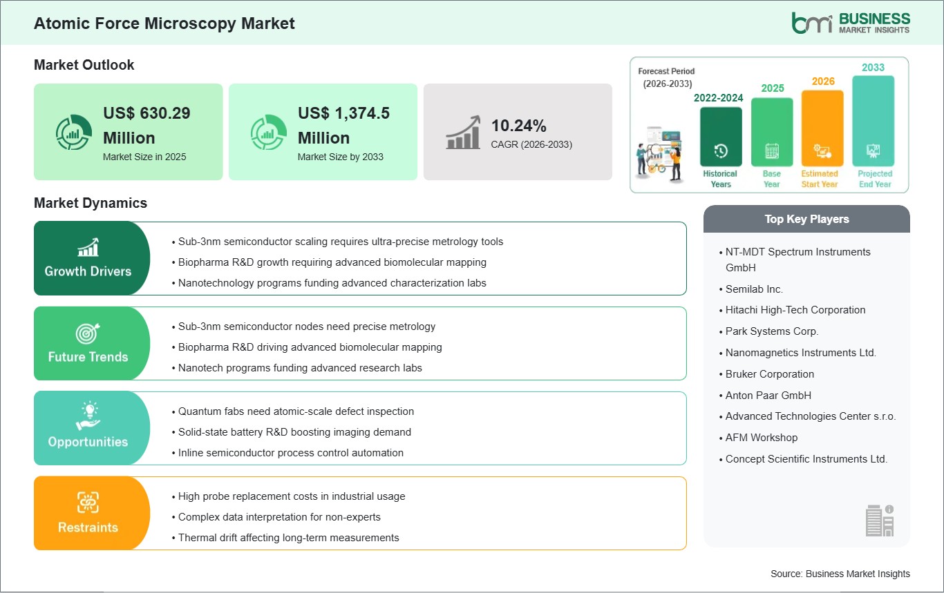
The Atomic Force Microscopy Market size is expected to reach US$ 1,374.5 Million by 2033 from US$ 630.29 Million in 2025. The market is estimated to record a CAGR of 10.24% from 2026 to 2033.
Executive Summary and Global Market Analysis:
The worldwide atomic force microscopy market is taking advantage of features like high-speed scanning probes, AI, assisted image analysis, and multimodal integration in order to achieve sub-nanometer resolution in semiconductor metrology and biomolecular imaging. These instruments unleash the full potential of piezoelectric actuators, true non-contact modes, and machine learning algorithms, providing throughput up to 10 times faster than traditional contact, mode AFMs. Therefore, leading fabs, biopharma labs, and 2D materials research can be done at defect-free nanoscale precision. Apart from the biggest benefits, a 50% reduction in tip wear compared to silicon probes, a 30% decrease in footprint by using compact scanners, and cloud-based data zoning have been turning atomic force microscopy into a vital instrument in human-centric nanotech, edge AI metrology, and sustainable electronics ecosystems. 6G, enabled nano, sensors, quantum computing requirements, and VR/AR simulation labs will be among the new beneficiaries of a strong surge due to the unstructured nanoscale data explosion.
The market is driven by national nanotech initiatives such as the US National Nanotechnology Initiative and lower costs of carbon nanotube probes. However, supply chain disruptions of high-purity piezo ceramics and interoperability issues with SEM/TEM protocols are becoming industry pain points. In addition, there is great potential in hybrid scanning tips, 1 nm resolution arrays, and battery electrolyte mapping networks.
Atomic Force Microscopy Market - Strategic Insights:
Get more information on this report
Atomic Force Microscopy Market Segmentation Analysis:
Key segments shaping the global atomic force microscopy market include offering, installation, types, and end user.
By offering, the market segments into Probes, Atomic Force Microscopes, and Others. The Probes segment dominated in 2025, optimized for high-throughput replacement in industrial workflows.
By grade, divisions cover Research and Industrial. The Industrial segment led in 2025, driven by quality control demands in fabs.
By application, segments are Nanotechnology, Material Science, Academics, Semiconductor & Electronics, and Others. The Semiconductor & Electronics segment held the top share in 2025, ideal for sub-5nm node inspection.
Atomic Force Microscopy Market Drivers and Opportunities:
Semiconductor Metrology Fuels Precision Boom
The atomic force microscopy segment was majorly influenced by hyperscale fabs upgrading their old SEMs with AI, optimized PeakForce tapping, and the operators were mostly concentrated on low, noise, tunable cantilevers from 0.1, 10 N/m springs. Bruker and Park Systems Dimension instruments are used along with Nanosurf controls for quantum dot arrays, giving rise to 40% yield improvements through sub-1 nm roughness mapping over 300mm wafers, which is crucial for EUV hybrid workforces.
In the frame of CHIPS Act rules, a 25% annual probe upgrade rate is leading to the accumulation of a backlog of more than 1M units by 2030. US labs are escalating CNT probes thanks to IRA incentives, with software analytics blending stressed phosphor chains in OLED picking. Hybrid tips glow in 150 battery bays, DAC, to AFM swaps give quick Return on Investment (ROI); thus, atomic systems will be the stepping stone for zero-touch mesh networks capable of holding exabytes, scale molecular models, liquid, cooled scanners, and PUE targets below 1.05.
Chip shortages originating from Taiwan's political tensions have brought attention to the importance of grid resilience. Thus, hybrid sensor arrays incorporating force, conductivity, and modulus monitors are able to prevent over-scanning in foundries that are threatened by adversaries. GaN scanners are the most suited ones in EMI, intensive EV plants, and for Noise Ratio (SNR) increased by more than 30% as compared to silicon competitors.
Life Sciences and Nano-IoT Open New Frontiers
Probes and AFMs are highly likely to be impacted positively by biopharma wellness booms and also by cockpits of Industry 5.0, thus allowing scope to cryogenic cove imaging and zonal robotics. Matter, like standards, enables the fusion of industrial tips with Thread for remote monitoring, thus the lab wiring is reduced by 60% compared to the legacy STMs for CES/Expo streams. On the other hand, consumer mandates like EU Nano, safety push probes to below $50/unit. Simultaneously, the call for autonomy demands 100 nm/s research links at less than US$ 100k/unit. The micro tips in scale become 5 nm, thereby cutting the BOMs for edge gateways by half. Industrial verticals apply research, grade in 48V DC grids as per UL standards. These developments, in effect, are positioning suppliers to seize US$ 400 million deals through 2034, with atomic force microscopy as pluggable cores for disaggregated IoT and immersive nano environments.
Atomic Force Microscopy Market Size and Share Analysis:
By offering, the global atomic force microscopy market is segments into Probes, Atomic Force Microscopes, and Others. The Probes segment dominated in 2025. Drives 45% installations: high-replacement scalability boosts fab wellness adoption in sub-3nm nodes.
By grade, the segments are Research and Industrial. The Industrial segment led in 2025. Captures 55% volume; automation programs demand rapid fab-to-industrial scaling.
By application, divisions include Nanotechnology, Material Science, Academics, Semiconductor & Electronics, and Others. The Semiconductor & Electronics segment held the largest share in 2025. Versatile 0.1-50 nm support enables seamless zone migrations globally.
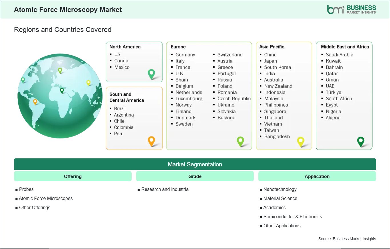
Australia, China, India, Japan, South Korea, Indonesia, Malaysia, Philippines, Singapore, Thailand, Vietnam, Bangladesh, New Zealand, Taiwan
South and Central America
Brazil, Argentina, Peru, Chile, Colombia
Middle East and Africa
Bahrain, Kuwait, Oman, Qatar, Saudi Arabia, United Arab Emirates, Turkiye, South Africa, Egypt, Algeria, Nigeria
Market leaders and key company profiles
NT-MDT Spectrum Instruments GmbH
Semilab Inc.
Hitachi High-Tech Corporation
Park Systems Corp.
Nanomagnetics Instruments Ltd.
Bruker Corporation
Anton Paar GmbH
Advanced Technologies Center s.r.o.
AFM Workshop
Concept Scientific Instruments Ltd.
Get more information on this report
Atomic Force Microscopy Market Report Coverage and Deliverables:
The "Atomic Force Microscopy Market Size and Forecast (2022 - 2033)" report provides a detailed analysis of the market covering below areas:
Atomic force microscopy market size and forecast at global, regional, and country levels for all the key market segments covered under the scope
Atomic force microscopy market trends, as well as market dynamics such as drivers, restraints, and key opportunities
Atomic force microscopy market analysis covering key market trends, global and regional framework, major players, regulations, and recent market developments
Industry landscape and competition analysis covering market concentration, heat map analysis, prominent players, and recent developments for the Atomic force microscopy market
Detailed company profiles, including SWOT analysis
Atomic Force Microscopy Market Geographic Insights:
The geographical scope of the atomic force microscopy market report is divided into five regions: North America, Asia Pacific, Europe, the Middle East & Africa, and South & Central America. The atomic force microscopy market in North America registered the highest market share in 2025.
North America still leads with mega-fabs and nano-labs across the US, Canada, and Mexico. There is a massive increase in US deployments, where sub-nm probes power TSMC's Arizona hubs and Intel edge nodes for tactical nano-AI. In Canada, operators like the National Research Council install research controls for ML pipelines. Maquiladoras light industrial AFMs to Tier 1 fab levels in Mexico. Europe advances via Horizon Europe and net-zero mandates, Germany's Zeiss and Tridonic craft probes for edge factories, the UK's Oxford cove adopted for BBC studios, and France's CEA stresses low-noise scanners for sovereign clouds. The Middle East builds data havens like Saudi NEOM's Aramco grids and UAE du's track probes for 6G sites. Asia Pacific thrives with China's 15th Plan trials and chip goals, TSMC taking micro-probe controls. Reliance in India deploys 1 nm/w retrofits but lags due to ceramic gaps. South and Central America will develop over the forecast period.
Get more information on this report
Atomic Force Microscopy Market Research Report Guidance:
The report includes qualitative and quantitative data in the atomic force microscopy market across offering, grade, application, and geography.
The report starts with the key takeaways (chapter 2), highlighting the key trends and outlook of the Atomic force microscopy market.
Chapter 3 includes the research methodology of the study.
Chapter 4 further includes ecosystem analysis.
Chapter 5 highlights the major industry dynamics in the Atomic force microscopy market, including factors that are driving the market, prevailing deterrents, potential opportunities, as well as future trends. Impact analysis of these drivers and restraints is also covered in this section.
Chapter 6 discusses the atomic force microscopy market scenario, in terms of historical market revenues, and forecast till the year 2031.
Chapters 7 to 10 cover the atomic force microscopy market segments by offering, grade, application, and geography across North America, Europe, Asia Pacific, the Middle East and Africa, and South and Central America. They cover the market volume, revenue forecast and factors driving the market.
Chapter 11 describes the competitive analysis along with the heat map analysis for the key players operating in the market.
Chapter 12 describes the industry landscape analysis. It provides detailed descriptions of business activities such as market initiatives, new developments, mergers, and joint ventures globally, along with a competitive landscape.
Chapter 13 provides detailed profiles of the major companies operating in the Atomic force microscopy market. Companies have been profiled on the basis of their key facts, business descriptions, products and services, financial overview, SWOT analysis, and key developments.
Chapter 14, i.e., the appendix, is inclusive of a brief overview of the company, a list of abbreviations, and a disclaimer.
Atomic Force Microscopy Market News and Key Development:
The atomic force microscopy market is evaluated by gathering qualitative and quantitative data post-primary and secondary research, which includes important corporate publications, association data, and databases. A few of the key developments in the atomic force microscopy market are:
In June 2025, Park Systems, a global leader in atomic force microscopy (AFM), successfully hosted a global interactive online showcase for the Park FX Large Sample AFM Series, bringing together a worldwide audience for an in-depth exploration of its advanced metrology solutions. The event highlighted Park’s most recent additions to its AFM product family, including the Park FX200, FX300, FX200 IR, and FX300 IR, through live-streamed demonstrations and simultaneous multilingual breakout sessions.
In May 2025, Oxford Instruments will introduce the Jupiter Discovery Atomic Force Microscope (AFM) to deliver best-in-class performance and exceptional ease of use. This versatile, large-sample AFM ensures that scientists in both academia and industry can attain the higher resolution, repeatability, and throughput they require while empowering even users with minimal training to achieve their research goals.
Key Sources Referred:
National Nanotechnology Initiative (NNI)International Electrotechnical Commission (IEC)SEMI StandardsNational Institutes of Health (NIH)World Bank - Global Trade IndicatorsWorld Trade Organization (WTO)International Trade Administration (ITA)Company websitesCompany annual reportsCompany investor presentations
The List of Companies - Atomic Force Microscopy Market
NT-MDT Spectrum Instruments
Semilab Inc.
Hitachi High-Technologies Corp (HHT)
Park Systems
Nanomagnetics Instruments
Bruker Corporation
Anton Paar
Advanced Technologies Center
AFM Workshop
Concept Scientific Instruments
About Author— Electronics and Semiconductor Research Team
Siddhika is an experienced market research professional with over five years of expertise in delivering actionable market intelligence and strategic insights to support business growth and decision-making. She has strong experience in designing and managing end-to-end research engagements, including research planning, data collection, and insight generation.
Proficient in research methodologies, Siddhika synthesizes diverse information sources to deliver accurate, high-quality insights and strategic recommendations. She excels at translating complex market information into strategic narratives that support executive decision-making..
Show More
Frequently Asked Questions
How big is the Atomic Force Microscopy Market?
The Atomic Force Microscopy Market is valued at US$ 630.29 Million in 2025, it is projected to reach US$ 1,374.5 Million by 2033.
What is the CAGR for Atomic Force Microscopy Market by (2026 - 2033)?
As per our report Atomic Force Microscopy Market, the market size is valued at US$ 630.29 Million in 2025, projecting it to reach US$ 1,374.5 Million by 2033. This translates to a CAGR of approximately 10.24% during the forecast period.
What segments are covered in this report?
The Atomic Force Microscopy Market report typically cover these key segments-
Offering (Probes, Atomic Force Microscopes, Other Offerings)
Grade (Research, Industrial)
Application (Nanotechnology, Material Science, Academics, Semiconductor & Electronics, Other Applications)
What is the historic period, base year, and forecast period taken for Atomic Force Microscopy Market?
The historic period, base year, and forecast period can vary slightly depending on the specific market research report. However, for the Atomic Force Microscopy Market report:
Historic Period : 2022-2024
Base Year : 2025
Forecast Period : 2026-2033
Who are the major players in Atomic Force Microscopy Market?
The Atomic Force Microscopy Market is populated by several key players, each contributing to its growth and innovation. Some of the major players include:
NT-MDT Spectrum Instruments GmbH
Semilab Inc.
Hitachi High-Tech Corporation
Park Systems Corp.
Nanomagnetics Instruments Ltd.
Bruker Corporation
Anton Paar GmbH
Advanced Technologies Center s.r.o.
AFM Workshop
Concept Scientific Instruments Ltd.
Who should buy this report?
The Atomic Force Microscopy Market report is valuable for diverse stakeholders, including:
Investors: Provides insights for investment decisions pertaining to market growth, companies, or industry insights. Helps assess market attractiveness and potential returns.
Industry Players: Offers competitive intelligence, market sizing, and trend analysis to inform strategic planning, product development, and sales strategies.
Suppliers and Manufacturers: Helps understand market demand for components, materials, and services related to concerned industry.
Researchers and Consultants: Provides data and analysis for academic research, consulting projects, and market studies.
Financial Institutions: Helps assess risks and opportunities associated with financing or investing in the concerned market.
Essentially, anyone involved in or considering involvement in the Atomic Force Microscopy Market value chain can benefit from the information contained in a comprehensive market report.


 Get Free Sample For Atomic Force Microscopy Market


