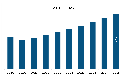
The semiconductor bonding market in Europe is expected to grow from US$ 215.77 million in 2022 to US$ 349.17 million by 2028. It is estimated to grow at a CAGR of 8.4% from 2022 to 2028.
Rising Adoption of Stacked Die Technology in IoT Devices
Due to the OEM’s increased need for enhanced capabilities and performance in smaller printed circuit boards (PCBs), the adoption of stacked die technology has grown in various electronic applications such as IoT and mobile devices. Stacked die refers to the placement of one chip on top of another or a spacer instead of the chip, followed by another chip. Sets of many rows of wire bonding loops are arranged, with each set connecting to a different die or spacer. Hence, remaining space after stacked die is used to fit many functionalities into a small die placement area. Thus, using stacked die technology to place the circuitry helps preserve valuable PCB space. Due to the limited workspace that PCB assembly and manufacturing companies witnessed with such extremely rigid and rigid-flex circuits, the demand for stacked die technology in IoT device is increasing. Moreover, the usage of stacked die significantly enhances design processes of semiconductor. The stacked die technology is used to produce a small-sized final design. One of the main factors causing the stacked die technique to advance is handheld electronic devices. Also, live tracking IoT gadget cannot be huge either. By reducing the amount of design effort and raising the likelihood of first-time success, time to market is reduced. Thus, the increasing adoption of stacked die technology in IoT devices is raising the demand for semiconductor bonding solutions in the market. In addition, OEMs in the semiconductor sector are utilizing the benefits of IoT beyond connectivity. Sensors, RFID tags, smart beacons, smart meters, and distribution control systems are IoT devices and technologies that are increasingly being used in various applications such as building and home automation, connected logistics, smart manufacturing, smart retail, smart mobility, and smart transportation. In Internet of Things (IoT) devices, semiconductor bonding techniques are utilized to compactly attach several stacked dies to substrates which will lead to the growth of the Europe semiconductor bonding market.
Market Overview
Germany, France, Italy, Russia, the UK, and rest of Europe are the key contributors to the semiconductor bonding market in the Europe. A stacked die is an assembly technique where two or more die is stacked and bonded in a single semiconductor package. It is used on a substrate having numerous functionalities around the same placement area. The performance of electrical devices is enhanced due to die piling. Thus, the utilization of stacked die is one of the major drivers accelerating the market growth. EV Group, HUTEM are a few of the prominent companies operating in the Europe semiconductor bonding market. These companies are majorly focusing on the market for MEMS sensors, CMOS image sensors, and RF devices. For instance, in March 2022, Merck KGaA, a Germany-based pharmaceutical company, announced a total investment of US$ 82 million to build a new semiconductor facility in Zhangjiagang, China. The growth of wafer bonding is fueled by the growing demand for various thermal imaging applications, including night vision systems for military and security use, imaging systems to improve building construction, thermal cameras for pedestrian protection systems in automobiles, and process monitoring systems for several commercial and industrial applications. MEMS manufacturers need advanced process equipment and expertise that will enable them to produce microbolometers at high throughput and yield for achieving the unit cost reductions required to meet the demand. The usage of EV Group’s (EVG) fully automated GEMINI wafer bonder provides cost-effective production of microbolometers. Similarly, in October 2020, in Austria, EVG established a complete process flow for combined die-to-wafer (D2W) hybrid and fusion bonding with sub-2μm placement accuracy for 3D semiconductor packaging.
Europe Semiconductor Bonding Market Revenue and Forecast to 2028 (US$ Million)
Based on type, the market is segmented into die bonder, wafer bonder, and flip chip bonder. The wafer bonder segment registered the largest market share in 2022.
Based on application, the market is segmented into RF devices, MEMS and sensors, LED, CMOS image sensors, and 3D NAND. The MEMS and sensors segment held a largest market share in 2022.
Based on country, the market is segmented into Germany, France, Italy, Russia, the UK, and rest of Europe. Germany dominated the market share in 2022.
ASMPT; DIAS Automation (HK) Ltd.; EV Group; HUTEM; Kulicke & Soffa Industries, Inc.; Palomar Technologies; Panasonic Corporation; Toray Industries Inc; WestBond, Inc.; and Yamaha Motor Corporation are the leading companies operating in the semiconductor bonding market in the Europe region.
Europe Semiconductor Bonding Market Strategic Insights
Get more information on this report
Europe Semiconductor Bonding Market Segmentation Analysis
Europe Semiconductor Bonding Market Report Highlights
Europe Semiconductor Bonding Report Scope
Report Attribute
Details
Market size in 2022
US$ 215.77 Million
Market Size by 2028
US$ 349.17 Million
CAGR (2022 - 2028)
8.4%
Historical Data
2020-2021
Forecast period
2023-2028
Segments Covered
By Type
Die Bonder
Wafer Bonder
Flip Chip Bonder
By Application
RF Devices
MEMS and Sensors
LED
CMOS Image Sensors
3D NAND
Regions and Countries Covered
Europe
UK, Germany, France, Russia, Italy, Rest of Europe
Market leaders and key company profiles
ASMPT
DIAS Automation (HK) Ltd.
EV Group
HUTEM
Kulicke & Soffa Industries, Inc.
Palomar Technologies
Panasonic Corporation
Toray Industries Inc
WestBond, Inc.
Yamaha Motor Corporation
Get more information on this report
Europe Semiconductor Bonding Market Country and Regional Insights
Get more information on this report
Identical Market Reports with other Region/Countries
The List of Companies - Europe Semiconductor Bonding Market
ASMPTDIAS Automation (HK) Ltd.EV GroupHUTEMKulicke & Soffa Industries, Inc.Palomar TechnologiesPanasonic CorporationToray Industries IncWestBond, Inc.Yamaha Motor Corporation
Frequently Asked Questions
How big is the Europe Semiconductor Bonding Market?
The Europe Semiconductor Bonding Market is valued at US$ 215.77 Million in 2022, it is projected to reach US$ 349.17 Million by 2028.
What is the CAGR for Europe Semiconductor Bonding Market by (2022 - 2028)?
As per our report Europe Semiconductor Bonding Market, the market size is valued at US$ 215.77 Million in 2022, projecting it to reach US$ 349.17 Million by 2028. This translates to a CAGR of approximately 8.4% during the forecast period.
What segments are covered in this report?
The Europe Semiconductor Bonding Market report typically cover these key segments-
Type (Die Bonder, Wafer Bonder, Flip Chip Bonder)
Application (RF Devices, MEMS and Sensors, LED, CMOS Image Sensors, 3D NAND)
What is the historic period, base year, and forecast period taken for Europe Semiconductor Bonding Market?
The historic period, base year, and forecast period can vary slightly depending on the specific market research report. However, for the Europe Semiconductor Bonding Market report:
Historic Period : 2020-2021
Base Year : 2022
Forecast Period : 2023-2028
Who are the major players in Europe Semiconductor Bonding Market?
The Europe Semiconductor Bonding Market is populated by several key players, each contributing to its growth and innovation. Some of the major players include:
ASMPT
DIAS Automation (HK) Ltd.
EV Group
HUTEM
Kulicke & Soffa Industries, Inc.
Palomar Technologies
Panasonic Corporation
Toray Industries Inc
WestBond, Inc.
Yamaha Motor Corporation
Who should buy this report?
The Europe Semiconductor Bonding Market report is valuable for diverse stakeholders, including:
Investors: Provides insights for investment decisions pertaining to market growth, companies, or industry insights. Helps assess market attractiveness and potential returns.
Industry Players: Offers competitive intelligence, market sizing, and trend analysis to inform strategic planning, product development, and sales strategies.
Suppliers and Manufacturers: Helps understand market demand for components, materials, and services related to concerned industry.
Researchers and Consultants: Provides data and analysis for academic research, consulting projects, and market studies.
Financial Institutions: Helps assess risks and opportunities associated with financing or investing in the concerned market.
Essentially, anyone involved in or considering involvement in the Europe Semiconductor Bonding Market value chain can benefit from the information contained in a comprehensive market report.


 Get Free Sample For Europe Semiconductor Bonding Market


