Analysis – by Type (Die Bonder, Wafer Bonder, and Flip Chip Bonder) and Application (RF Devices, MEMS and Sensors, LED, CMOS Image Sensors, and 3D NAND)
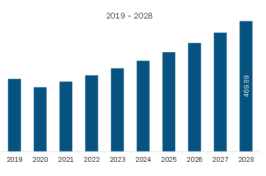
The semiconductor bonding market in Asia Pacific is expected to grow from US$ 274.55 million in 2022 to US$ 469.89 million by 2028. It is estimated to grow at a CAGR of 9.4% from 2022 to 2028.
Adoption of Die Bonding in Telecommunication
The growing demand for high-performance optical communication devices boosts 5G deployment and datacenter applications. Further, this supports 5G wireless fronthaul and next-generation Ethernet modules, which include 2x200GbE, 4x100GbE, 400GbE, and CWDM/DWDM transceivers. The demand for high-performance optical devices is also generating requirements for smaller packaging housing, rapid technology innovation, smaller chips/dies with higher density in the package, higher-volume manufacturing, quick product iterations, and an economical price point. The new requirements are also needed in lidar, AR/VR, advanced photonic sensors, MEMS, and highly integrated silicon photonics devices. For manufacturing all the above devices, successfully deploying flexible die bonding solutions with high post-bonding accuracy and great long-term stability is required. Various manufacturers are producing flexible high bonding solutions to meet this requirement. For instance, MRSI-HVM by MRSI Systems is a flexible high-speed die bonder which can achieve <±1.5 µm @ 3 sigma. Thus, with this, the company provides the best manufacturing solution for increasing volume and mix in manufacturing 5G and datacenter core devices.
Market Overview
Australia, China, India, Japan, South Korea, and rest of Asia Pacific are the key contributors to the semiconductor bonding market in the Asia Pacific. The market growth is attributed to the presence of several OSAT (Outsourced Semiconductor Assembly and Test) players in Taiwan and China. In February 2021, SMIC (Semiconductor Manufacturing International Co) announced the total investment of US$ 9.06 billion in Shanghai wafer plant with the government-backed China Integrated Circuit Industry Investment Fund. Similarly, in June 2020, GlobalWafers Co., Ltd invested US$ 339 million in its Taisil (Taiwan) branch to upsurge 300-mm silicon wafer capabilities. This enhanced capacity is projected to meet the growing demand for high-quality silicon wafers. Such developments in the region are driving the demand for wafer bonding devices. ASM Pacific Technology; DIAS Automation (HK) Ltd; Kulicke and Soffa Industries, Inc; Panasonic Corporation; SHINKAWA Electric Co., Ltd; and TORAY ENGINEERING Co. Ltd are a few of the prominent companies operating in the Asia Pacific semiconductor bonding market. These companies are majorly focusing on the market for MEMS sensors, LED sensors, and CMOS image sensors. The increasing number of Integrated Device Manufacturer (IDMs) and bulk manufacturing of electronic devices such as smart watches, mobile phones, and household appliances in China and Taiwan is projected to boost the market growth. For example, HANIMI Semiconductor Co. Ltd has launched its new Flip Chip Bonder-5.0. Its major focus is on high-end semiconductor production, which is propelling the demand for semiconductor bonding.
Asia Pacific Semiconductor Bonding Market Revenue and Forecast to 2028 (US$ Million)
Asia Pacific Semiconductor Bonding Market Segmentation
Based on type, the market is segmented into die bonder, wafer bonder, and flip chip bonder. The wafer bonder segment registered the largest market share in 2022.
Based on application, the market is segmented into RF devices, MEMS and sensors, LED, CMOS image sensors, and 3D NAND. The MEMS and sensors segment held a largest market share in 2022.
Based on country, the market is segmented into Australia, China, India, Japan, South Korea, and rest of Asia Pacific. Rest of Asia Pacific dominated the market share in 2022.
ASMPT; DIAS Automation (HK) Ltd.; EV Group; HUTEM; Kulicke & Soffa Industries, Inc.; Palomar Technologies; Panasonic Corporation; Toray Industries Inc; WestBond, Inc.; and Yamaha Motor Corporation are the leading companies operating in the semiconductor bonding market in the Asia Pacific region.
Asia Pacific Semiconductor Bonding Market Strategic Insights
Get more information on this report
Asia Pacific Semiconductor Bonding Market Segmentation Analysis
Asia Pacific Semiconductor Bonding Market Report Highlights
Asia Pacific Semiconductor Bonding Report Scope
Report Attribute
Details
Market size in 2022
US$ 274.55 Million
Market Size by 2028
US$ 469.89 Million
CAGR (2022 - 2028)
9.4%
Historical Data
2020-2021
Forecast period
2023-2028
Segments Covered
By Type
Die Bonder
Wafer Bonder
Flip Chip Bonder
By Application
RF Devices
MEMS and Sensors
LED
CMOS Image Sensors
3D NAND
Regions and Countries Covered
Asia-Pacific
China, India, Japan, Australia, Rest of Asia-Pacific
Market leaders and key company profiles
ASMPT
DIAS Automation (HK) Ltd.
EV Group
HUTEM
Kulicke & Soffa Industries, Inc.
Palomar Technologies
Panasonic Corporation
Toray Industries Inc
WestBond, Inc.
Yamaha Motor Corporation
Get more information on this report
Asia Pacific Semiconductor Bonding Market Country and Regional Insights
Get more information on this report
Identical Market Reports with other Region/Countries
The List of Companies - Asia Pacific Semiconductor Bonding Market
ASMPTDIAS Automation (HK) Ltd.EV GroupHUTEMKulicke & Soffa Industries, Inc.Palomar TechnologiesPanasonic CorporationToray Industries IncWestBond, Inc.Yamaha Motor Corporation
Frequently Asked Questions
How big is the Asia Pacific Semiconductor Bonding Market?
The Asia Pacific Semiconductor Bonding Market is valued at US$ 274.55 Million in 2022, it is projected to reach US$ 469.89 Million by 2028.
What is the CAGR for Asia Pacific Semiconductor Bonding Market by (2022 - 2028)?
As per our report Asia Pacific Semiconductor Bonding Market, the market size is valued at US$ 274.55 Million in 2022, projecting it to reach US$ 469.89 Million by 2028. This translates to a CAGR of approximately 9.4% during the forecast period.
What segments are covered in this report?
The Asia Pacific Semiconductor Bonding Market report typically cover these key segments-
Type (Die Bonder, Wafer Bonder, Flip Chip Bonder)
Application (RF Devices, MEMS and Sensors, LED, CMOS Image Sensors, 3D NAND)
What is the historic period, base year, and forecast period taken for Asia Pacific Semiconductor Bonding Market?
The historic period, base year, and forecast period can vary slightly depending on the specific market research report. However, for the Asia Pacific Semiconductor Bonding Market report:
Historic Period : 2020-2021
Base Year : 2022
Forecast Period : 2023-2028
Who are the major players in Asia Pacific Semiconductor Bonding Market?
The Asia Pacific Semiconductor Bonding Market is populated by several key players, each contributing to its growth and innovation. Some of the major players include:
ASMPT
DIAS Automation (HK) Ltd.
EV Group
HUTEM
Kulicke & Soffa Industries, Inc.
Palomar Technologies
Panasonic Corporation
Toray Industries Inc
WestBond, Inc.
Yamaha Motor Corporation
Who should buy this report?
The Asia Pacific Semiconductor Bonding Market report is valuable for diverse stakeholders, including:
Investors: Provides insights for investment decisions pertaining to market growth, companies, or industry insights. Helps assess market attractiveness and potential returns.
Industry Players: Offers competitive intelligence, market sizing, and trend analysis to inform strategic planning, product development, and sales strategies.
Suppliers and Manufacturers: Helps understand market demand for components, materials, and services related to concerned industry.
Researchers and Consultants: Provides data and analysis for academic research, consulting projects, and market studies.
Financial Institutions: Helps assess risks and opportunities associated with financing or investing in the concerned market.
Essentially, anyone involved in or considering involvement in the Asia Pacific Semiconductor Bonding Market value chain can benefit from the information contained in a comprehensive market report.


 Get Free Sample For Asia Pacific Semiconductor Bonding Market


