Analysis – Wafer Size (6 Inch, 8 Inch, 12 Inch, and Others), Application (LED, Power Semiconductor, and MEMS-Based Device), End User (Consumer Electronics, Automotive, Healthcare, Aerospace and Defense, and Others), and Type (Heteroepitaxy and Homoepitaxy)
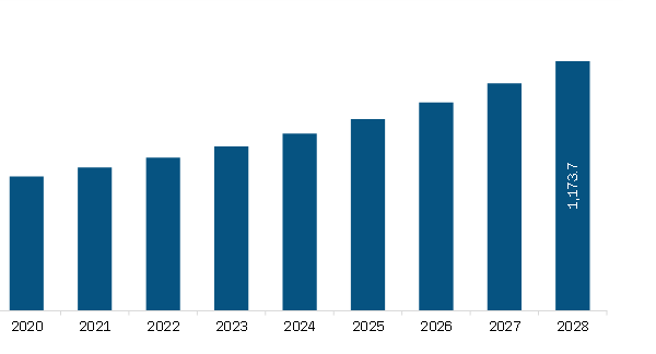
The North America silicon EPI wafer market is expected to grow from US$ 718.31 million in 2022 to US$ 1,173.68 million by 2028; it is estimated to grow at a CAGR of 8.5%from 2022 to 2028.
An epitaxial wafer, also known as an EPI wafer, is created by placing a layer of epitaxial silicon single crystal on a single crystal silicon wafer. This wafer helps regulate doping profiles that are difficult to manage using conventional techniques such as diffusion and ion implantation. Silicon epitaxial wafers are also the main component used in the production of various semiconductor devices that have applications in consumer, industrial, military, and space electronics. The wafers are used in bipolar and metal-oxide-semiconductor (MOS) integrated circuit (IC) substrates. They are also being used in diode and transistor elements. Silicon epitaxial wafers are used in energy-saving power gadgets and other devices with power sources. They are also used in LEDs, computers, tablets, cellphones, gyroscopes, and gaming consoles. Epiel, a specialized silicon epitaxial wafer manufacturer, provides epitaxial services for the semiconductor industry. The company offers a variety of custom silicon epitaxial wafers in sizes ranging from 3" (76 mm) to 8" (200 mm) for important microelectronics applications, including discrete power devices, integrated circuits, and sensors. In 2020, Qromis, a US-based start-up, signed a licensing arrangement with Japan's Shin-Etsu Chemical to produce substrates and epitaxial wafers for GaN power/RF electronics, LED devices, and other devices. The company has already made available 6-inch and 8-inch GaN-ready QST substrates and 6-inch and 8-inch "templates" with 5-inch and 10-inch micron GaN layers. It is developing 900V and 1200V GaN HEMT EPI wafers along with 200V and 650V GaN HEMT EPI wafers based on 6-inch and 8-inch QST substrates for electronic instruments. The business also intends to set up a second production facility for QST substrates and GaN-on-QST epitaxy wafers, considering the positive projections of GaN adoption due to growth of the silicon EPI wafer market.
Vendors in the North America silicon EPI wafer market can attract new customers and expand their footprints in emerging markets by providing innovative products enabled by new technologies. This is likely to drive the North America silicon EPI wafer market at a notable CAGR during the forecast period.
North America Silicon EPI Wafer Market Revenue and Forecast to 2028 (US$ Million)
North America Silicon EPI Wafer Market Segmentation
The North America silicon EPI wafer market is segmented on the basis of wafer size, application, end user, type, and country. Based on wafer size, the market is segmented into 6 inch, 8 inch, 12 inch, and others.Based on application, the market is divided into led, power semiconductor, and MEMS-based devices. By end user, the North America silicon EPI wafer market is segmented intoconsumer electronics, automotive, healthcare, aerospace and defense, and others. Based on type, the market is bifurcated into heteroepitaxy and homoepitaxy. Based on country, the North America silicon EPI wafer market is segmented into the US, Mexico, and Canada.
North America Silicon EPI Wafer Market —Companies Mentioned
Applied Materials, Inc.; II-VI Incorporated; Shin-Etsu Chemical Co., Ltd.; SUMCO CORPORATION; Wafer World Inc.; Siltronic AG; NICHIA CORPORATION; EpiGaN nv (Soitec Belgium N.V.); and SK Siltron Co., Ltd.are among the major companies operating in the North America silicon EPI wafer market.
North America Silicon EPI Wafer Market Strategic Insights
Get more information on this report
North America Silicon EPI Wafer Market Segmentation Analysis
North America Silicon EPI Wafer Market Report Highlights
North America Silicon EPI Wafer Report Scope
Report Attribute
Details
Market size in 2022
US$ 718.31 Million
Market Size by 2028
US$ 1,173.68 Million
CAGR (2022 - 2028)
8.5%
Historical Data
2020-2021
Forecast period
2023-2028
Segments Covered
By Wafer Size
6 Inch
8 Inch
12 Inch
By Application
LED
Power Semiconductor
MEMS-Based Device
By End User
Consumer Electronics
Automotive
Healthcare
Aerospace and Defense
By Type
Heteroepitaxy
Homoepitaxy
Regions and Countries Covered
North America
US, Canada, Mexico
Market leaders and key company profiles
Applied Materials, Inc.
II-VI Incorporated
Shin-Etsu Chemical Co., Ltd.
SUMCO CORPORATION
Wafer World Inc.
Siltronic AG
NICHIA CORPORATION
EpiGaN nv (Soitec Belgium N.V.)
SK Siltron Co., Ltd
Get more information on this report
North America Silicon EPI Wafer Market Country and Regional Insights
Get more information on this report
Identical Market Reports with other Region/Countries
The List of Companies - North America Silicon EPI Wafer Market
Applied Materials, Inc. II-VI Incorporated Shin-Etsu Chemical Co., Ltd. SUMCO CORPORATION Wafer World Inc. Siltronic AG NICHIA CORPORATION EpiGaN nv (Soitec Belgium N.V.) SK Siltron Co., Ltd
Frequently Asked Questions
How big is the North America Silicon EPI Wafer Market?
The North America Silicon EPI Wafer Market is valued at US$ 718.31 Million in 2022, it is projected to reach US$ 1,173.68 Million by 2028.
What is the CAGR for North America Silicon EPI Wafer Market by (2022 - 2028)?
As per our report North America Silicon EPI Wafer Market, the market size is valued at US$ 718.31 Million in 2022, projecting it to reach US$ 1,173.68 Million by 2028. This translates to a CAGR of approximately 8.5% during the forecast period.
What segments are covered in this report?
The North America Silicon EPI Wafer Market report typically cover these key segments-
Wafer Size (6 Inch, 8 Inch, 12 Inch)
Application (LED, Power Semiconductor, MEMS-Based Device)
End User (Consumer Electronics, Automotive, Healthcare, Aerospace and Defense)
Type (Heteroepitaxy, Homoepitaxy)
What is the historic period, base year, and forecast period taken for North America Silicon EPI Wafer Market?
The historic period, base year, and forecast period can vary slightly depending on the specific market research report. However, for the North America Silicon EPI Wafer Market report:
Historic Period : 2020-2021
Base Year : 2022
Forecast Period : 2023-2028
Who are the major players in North America Silicon EPI Wafer Market?
The North America Silicon EPI Wafer Market is populated by several key players, each contributing to its growth and innovation. Some of the major players include:
Applied Materials, Inc.
II-VI Incorporated
Shin-Etsu Chemical Co., Ltd.
SUMCO CORPORATION
Wafer World Inc.
Siltronic AG
NICHIA CORPORATION
EpiGaN nv (Soitec Belgium N.V.)
SK Siltron Co., Ltd
Who should buy this report?
The North America Silicon EPI Wafer Market report is valuable for diverse stakeholders, including:
Investors: Provides insights for investment decisions pertaining to market growth, companies, or industry insights. Helps assess market attractiveness and potential returns.
Industry Players: Offers competitive intelligence, market sizing, and trend analysis to inform strategic planning, product development, and sales strategies.
Suppliers and Manufacturers: Helps understand market demand for components, materials, and services related to concerned industry.
Researchers and Consultants: Provides data and analysis for academic research, consulting projects, and market studies.
Financial Institutions: Helps assess risks and opportunities associated with financing or investing in the concerned market.
Essentially, anyone involved in or considering involvement in the North America Silicon EPI Wafer Market value chain can benefit from the information contained in a comprehensive market report.


 Get Free Sample For North America Silicon EPI Wafer Market


