Analysis – Wafer Size (6 Inch, 8 Inch, 12 Inch, and Others), Application (LED, Power Semiconductor, and MEMS-Based Device), End User (Consumer Electronics, Automotive, Healthcare, Aerospace and Defense, and Others), and Type (Heteroepitaxy and Homoepitaxy)
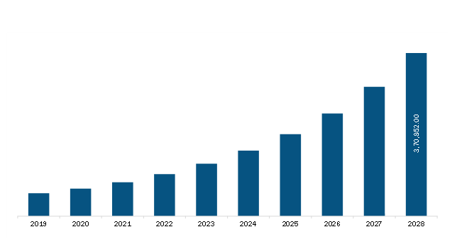
The Asia Pacific silicon EPI wafer market is expected to grow from US$ 1,635.16 million in 2022 to US$ 2,820.99 million by 2028; it is estimated to grow at a CAGR of 9.5% from 2022 to 2028.
Gallium nitride (GaN), a wide bandgap semiconductor, supports the functioning of devices at higher temperatures and voltages than silicon-based devices. The greater dielectric breakdown of GaN also makes it possible to build smaller devices with lower resistance. Lower resistance leads to smaller devices with less capacitance (on). Epitaxial GaN wafers, characterized by high efficiency and high-power output, are a base material used in power and radio frequency (RF) devices. They are used in defense radars, electric car power converters, 5G base stations, and quick chargers for IT devices. For instance, IVWorks, South Korea, makes GaN epitaxial wafers a crucial component of DC power devices and 5G communication devices by using deep learning-based artificial intelligence (AI) epitaxy technology, further attracting a US$ 6.7 million Series B investment. Due to their high electron mobility, current density, and breakdown voltage, GaN can be used to create high-efficiency, high-output power devices that operate at a high frequency. It is smaller, quicker, and more efficient than Si, SiC, and GaAs materials, and produces more power than these materials. GaN epitaxial growth is necessary on a heterogeneous substrate since GaN has not yet been adequately developed in free-standing wafer technology, unlike Si, SiC, and GaAs (Si or SiC). Although Si can affordably handle wafers with enormous diameters, a technique to manage stress and defect density is required because of the huge lattice mismatch and thermal expansion coefficient difference from GaN. Continuous advancements in AI-based GaN wafers are providing lucrative opportunities for the future growth of the silicon EPI wafer market.
Vendors in the Asia-Pacific silicon EPI wafer market can attract new customers and expand their footprints in emerging markets by providing innovative products. This is likely to drive market at a notable CAGR during the forecast period.
The Asia-Pacific Silicon EPI Wafer Market Revenue and Forecast to 2028 (US$ Million)
The Asia-Pacific silicon EPI wafer market is segmented on the basis of wafer size, application, end user, type, and country. Based on wafer size, the market is segmented into 6 inch, 8 inch, 12 inch, and others. Based on application, the market is divided into led, power semiconductor, and MEMS-based devices. By end user, the Asia-Pacific silicon EPI wafer market is segmented into consumer electronics, automotive, healthcare, aerospace and defense, and others. Based on type, the market is bifurcated into heteroepitaxy and homoepitaxy. Based on country, the Asia Pacific silicon EPI wafer market is segmented into Taiwan, China, India, Japan, South Korea, and Rest of Asia Pacific.
Asia Pacific Silicon EPI Wafer Market — Companies Mentioned
Applied Materials, Inc.; II-VI Incorporated; Shin-Etsu Chemical Co., Ltd.; SUMCO CORPORATION; Siltronic AG; NICHIA CORPORATION; GlobalWafers Japan Co., Ltd.; EpiGaN nv (Soitec Belgium N.V.) and SK Siltron Co., Ltd. are among the major companies operating in the Asia-Pacific silicon EPI wafer market.
Asia Pacific Silicon EPI Wafer Market Strategic Insights
Get more information on this report
Asia Pacific Silicon EPI Wafer Market Segmentation Analysis
Asia Pacific Silicon EPI Wafer Market Report Highlights
Asia Pacific Silicon EPI Wafer Report Scope
Report Attribute
Details
Market size in 2022
US$ 1,635.16 Million
Market Size by 2028
US$ 2,820.99 Million
CAGR (2022 - 2028)
9.5%
Historical Data
2020-2021
Forecast period
2023-2028
Segments Covered
By Wafer Size
6 Inch
8 Inch
12 Inch
By Application
LED
Power Semiconductor
MEMS-Based Device
By End User
Consumer Electronics
Automotive
Healthcare
Aerospace and Defense
By Type
Heteroepitaxy
Homoepitaxy
Regions and Countries Covered
Asia-Pacific
China, India, Japan, Australia, Rest of Asia-Pacific
Market leaders and key company profiles
Applied Materials, Inc.
II-VI Incorporated
Shin-Etsu Chemical Co., Ltd.
SUMCO CORPORATION
Siltronic AG
NICHIA CORPORATION
GlobalWafers Japan Co., Ltd.
EpiGaN nv (Soitec Belgium N.V.)
SK Siltron Co., Ltd
Get more information on this report
Asia Pacific Silicon EPI Wafer Market Country and Regional Insights
Get more information on this report
Identical Market Reports with other Region/Countries
The List of Companies - Asia Pacific Silicon EPI Wafer Market
Applied Materials, Inc. II-VI Incorporated Shin-Etsu Chemical Co., Ltd. SUMCO CORPORATION Siltronic AG NICHIA CORPORATION GlobalWafers Japan Co., Ltd. EpiGaN nv (Soitec Belgium N.V.) SK Siltron Co., Ltd
Frequently Asked Questions
How big is the Asia Pacific Silicon EPI Wafer Market?
The Asia Pacific Silicon EPI Wafer Market is valued at US$ 1,635.16 Million in 2022, it is projected to reach US$ 2,820.99 Million by 2028.
What is the CAGR for Asia Pacific Silicon EPI Wafer Market by (2022 - 2028)?
As per our report Asia Pacific Silicon EPI Wafer Market, the market size is valued at US$ 1,635.16 Million in 2022, projecting it to reach US$ 2,820.99 Million by 2028. This translates to a CAGR of approximately 9.5% during the forecast period.
What segments are covered in this report?
The Asia Pacific Silicon EPI Wafer Market report typically cover these key segments-
Wafer Size (6 Inch, 8 Inch, 12 Inch)
Application (LED, Power Semiconductor, MEMS-Based Device)
End User (Consumer Electronics, Automotive, Healthcare, Aerospace and Defense)
Type (Heteroepitaxy, Homoepitaxy)
What is the historic period, base year, and forecast period taken for Asia Pacific Silicon EPI Wafer Market?
The historic period, base year, and forecast period can vary slightly depending on the specific market research report. However, for the Asia Pacific Silicon EPI Wafer Market report:
Historic Period : 2020-2021
Base Year : 2022
Forecast Period : 2023-2028
Who are the major players in Asia Pacific Silicon EPI Wafer Market?
The Asia Pacific Silicon EPI Wafer Market is populated by several key players, each contributing to its growth and innovation. Some of the major players include:
Applied Materials, Inc.
II-VI Incorporated
Shin-Etsu Chemical Co., Ltd.
SUMCO CORPORATION
Siltronic AG
NICHIA CORPORATION
GlobalWafers Japan Co., Ltd.
EpiGaN nv (Soitec Belgium N.V.)
SK Siltron Co., Ltd
Who should buy this report?
The Asia Pacific Silicon EPI Wafer Market report is valuable for diverse stakeholders, including:
Investors: Provides insights for investment decisions pertaining to market growth, companies, or industry insights. Helps assess market attractiveness and potential returns.
Industry Players: Offers competitive intelligence, market sizing, and trend analysis to inform strategic planning, product development, and sales strategies.
Suppliers and Manufacturers: Helps understand market demand for components, materials, and services related to concerned industry.
Researchers and Consultants: Provides data and analysis for academic research, consulting projects, and market studies.
Financial Institutions: Helps assess risks and opportunities associated with financing or investing in the concerned market.
Essentially, anyone involved in or considering involvement in the Asia Pacific Silicon EPI Wafer Market value chain can benefit from the information contained in a comprehensive market report.


 Get Free Sample For Asia Pacific Silicon EPI Wafer Market


