Europe Semiconductor Metrology and Inspection Market Forecast to 2028 – COVID-19 Impact and Regional Analysis – by Type (Wafer Inspection System, Mask Inspection System, and Thin Film Metrology), Technology (Optical and E-Beam), and Organization Size (Large Enterprises and SMEs)    

BMIRE00027261 | Pages: 125 | Electronics and Semiconductor | Oct 2022 | Type: Regional | Status: Published

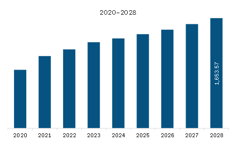
The Europe semiconductor metrology and inspection market is expected to grow from US$ 1,187.08 million in 2022 to US$ 1,653.57 million by 2028; it is estimated to grow at a CAGR of 4.8% from 2022 to 2028.


 Wafer fabrication, manufacturing, and other procedures use advanced packaging (AP) technology. Controlling these operations in the back end necessitates inspection and measurement methods. Shrinking feature sizes are driving the demand for high accuracy, precision, sensitivity, and throughput. On the other hand, AP procedures face measurement and inspection issues, such as bump metrology and nonvisual flaws, that are unique to back-end applications. Special requirements, combined with the increased diversity and rapid evolution of AP processes, propel the demand for flexible measurement and inspection systems that can control a wide range of parameters, including two-dimensional (2D) and three-dimensional (3D) geometries, and can be adapted to new requirements as they arise. Combining various competencies into a single platform is the most economical and effective use of capital. Keeping up with the industry's roadmap necessitates novel solutions from equipment providers focusing on the unique requirements of AP operations. For example, KLA Corporation offers Kronos 1190 patterned wafer inspection system with high-resolution optics in advanced wafer-level packaging (AWLP) applications such as 3D IC and high-density fan-out. The system gives sensitivity to important flaws for process development and production monitoring. Manufacturers are under pressure to improve quality and dependability. This is especially true in industries such as automotive, where consumer safety is a major concern. Thousands of semiconductor components exist in autos. In addition, the number of components might increase by orders of magnitude in completely driverless vehicles. For a car with 10,000 components, a component failure rate of one in a million amounts to a vehicle failure rate of one in 100, which is unacceptable. To meet this challenge in current and next-generation packages, defect sensitivity down to the micrometer level and the ability to discern lethal faults swiftly and consistently amid massive raw data streams are required. Gauge repeatability and reproducibility (R&R) investigations are becoming relevant. Engineers need technologies to turn raw data into useful process knowledge. E-beam technology is also being adopted in advanced packaging. Electrons are created within the tool in an e-beam inspection system and then hit the surface of a die. The electrons scatter and bounce back to a detector, allowing it to detect chips with faults.


With the new features and technologies, vendors can attract new customers and expand their footprints in emerging markets. This factor is likely to drive the Europe semiconductor metrology and inspection market. The Europe semiconductor metrology and inspection market is expected to grow at a good CAGR during the forecast period.     


 Europe Semiconductor Metrology and Inspection Market Revenue and Forecast to 2028 (US$ Million)        

 Europe Semiconductor Metrology and Inspection Market Revenue and Forecast to 2028 (US$ Million)        

Get more information on this report :


Europe Semiconductor Metrology and Inspection Market Segmentation       


The Europe semiconductor metrology and inspection market is segmented based on type, technology, organization size, and country. Based on type, the Europe semiconductor metrology and inspection market is segmented into wafer inspection system, mask inspection system, and thin film metrology. The wafer inspection system segment dominated the market in 2022. Based on technology, the Europe semiconductor metrology and inspection market is bifurcated into optical and e-beam. The optical segment dominated the market in 2022. Based on organization size, the Europe semiconductor metrology and inspection market is bifurcated into large enterprises and SMEs. The large enterprises segment dominated the market in 2022. Based on country, the Europe semiconductor metrology and inspection market has been segmented into the UK, Germany, France, Italy, Russia, and the Rest of Europe. Germany dominated the market in 2022.      


Applied Materials, Inc.; ASML Holding N.V.; Hitachi High-Tech Corporation; JEOL Ltd; KLA Corporation; Lasertec Corporation; Nikon Metrology NV; Nova Ltd.; Onto Innovation; and Thermo Fisher Scientific Inc. are among the leading companies in the Europe semiconductor metrology and inspection market.   

1.           Introduction

1.1         Study Scope

1.2         The Insight Partners Research Report Guidance

1.3         Market Segmentation

2.           Key Takeaways

3.        Research Methodology

3.1         Coverage

3.2         Secondary Research

3.3         Primary Research

4.           Europe Semiconductor Metrology and Inspection Market Landscape

4.1         Market Overview

4.2         Europe PEST Analysis

4.3         Ecosystem Analysis

4.4         Expert Opinion

5.           Europe Semiconductor Metrology and Inspection Market – Key Market Dynamics

5.1         Market Drivers

5.1.1        Escalating Use of Metrology and Inspection for Advanced Packaging Processes

5.1.2        Increasing Number of Semiconductor Applications

5.2         Market Restraints

5.2.1        High Setup Cost of Metrology and Inspection Equipment

5.3         Future Trends

5.3.1        Increasing Use of AI in Metrology and Inspection Systems

5.4         Impact Analysis of Drivers and Restraints

6.           Semiconductor Metrology and Inspection Market – Europe Analysis

6.1         Europe Semiconductor Metrology and Inspection Market Overview

6.2         Europe Semiconductor Metrology and Inspection Market – Revenue and Forecast to 2028 (US$ Million)

7.           Europe Semiconductor Metrology and Inspection Market Analysis – By Type

7.1         Overview

7.2         Europe Semiconductor Metrology and Inspection Market, By Type (2021 and 2028)

7.3         Wafer Inspection System

7.3.1        Overview

7.3.2        Wafer Inspection System: Semiconductor Metrology and Inspection Market – Revenue, and Forecast to 2028 (US$ Million)

7.4         Mask Inspection System

7.4.1        Overview

7.4.2        Mask Inspection System: Semiconductor Metrology and Inspection Market – Revenue, and Forecast to 2028 (US$ Million)

7.5         Thin Film Metrology

7.5.1        Overview

7.5.2        Thin Film Metrology: Semiconductor Metrology and Inspection Market – Revenue, and Forecast to 2028 (US$ Million)

8.           Europe Semiconductor Metrology and Inspection Market Analysis – By Technology

8.1         Overview

8.2         Europe Semiconductor Metrology and Inspection Market, By Technology (2021 and 2028)

8.3         Optical

8.3.1        Overview

8.3.2        Optical: Semiconductor Metrology and Inspection Market – Revenue, and Forecast to 2028 (US$ Million)

8.4         E-Beam

8.4.1        Overview

8.4.2        E-Beam: Semiconductor Metrology and Inspection Market – Revenue, and Forecast to 2028 (US$ Million)

9.           Europe Semiconductor Metrology and Inspection Market Analysis – By Organization Size

9.1         Overview

9.2         Europe Semiconductor Metrology and Inspection Market, By Organization Size (2021 and 2028)

9.3         Large Enterprises

9.3.1        Overview

9.3.2        Large Enterprises: Semiconductor Metrology and Inspection Market – Revenue and Forecast to 2028 (US$ Million)

9.4         SMEs

9.4.1        Overview

9.4.2        SMEs: Semiconductor Metrology and Inspection Market – Revenue and Forecast to 2028 (US$ Million)

10.        Europe Semiconductor Metrology and Inspection Market – Country Analysis

10.1      Overview

10.1.1     Europe Semiconductor Metrology and Inspection Market Breakdown, by Country

10.1.1.1       Germany Semiconductor Metrology and Inspection Market, Revenue and Forecast to 2028

10.1.1.1.1       Germany Semiconductor Metrology and Inspection Market Breakdown, By Type

10.1.1.1.2       Germany Semiconductor Metrology and Inspection Market Breakdown, By Technology

10.1.1.1.3       Germany Semiconductor Metrology and Inspection Market Breakdown, By Organization Size

10.1.1.2       France Semiconductor Metrology and Inspection Market, Revenue and Forecast to 2028

10.1.1.2.1       France Semiconductor Metrology and Inspection Market Breakdown, By Type

10.1.1.2.2       France Semiconductor Metrology and Inspection Market Breakdown, By Technology

10.1.1.2.3       France Semiconductor Metrology and Inspection Market Breakdown, By Organization Size

10.1.1.3       Italy Semiconductor Metrology and Inspection Market, Revenue and Forecast to 2028

10.1.1.3.1       Italy Semiconductor Metrology and Inspection Market Breakdown, By Type

10.1.1.3.2       Italy Semiconductor Metrology and Inspection Market Breakdown, By Technology

10.1.1.3.3       Italy Semiconductor Metrology and Inspection Market Breakdown, By Organization Size

10.1.1.4       UK Semiconductor Metrology and Inspection Market, Revenue and Forecast to 2028

10.1.1.4.1       UK Semiconductor Metrology and Inspection Market Breakdown, By Type

10.1.1.4.2       UK Semiconductor Metrology and Inspection Market Breakdown, By Technology

10.1.1.4.3       UK Semiconductor Metrology and Inspection Market Breakdown, By Organization Size

10.1.1.5       Russia Semiconductor Metrology and Inspection Market, Revenue and Forecast to 2028

10.1.1.5.1       Russia Semiconductor Metrology and Inspection Market Breakdown, By Type

10.1.1.5.2       Russia Semiconductor Metrology and Inspection Market Breakdown, By Technology

10.1.1.5.3       Russia Semiconductor Metrology and Inspection Market Breakdown, By Organization Size

10.1.1.6       Rest of Europe Semiconductor Metrology and Inspection Market, Revenue and Forecast to 2028

10.1.1.6.1       Rest of Europe Semiconductor Metrology and Inspection Market Breakdown, By Type

10.1.1.6.2       Rest of Europe Semiconductor Metrology and Inspection Market Breakdown, By Technology

10.1.1.6.3       Rest of Europe Semiconductor Metrology and Inspection Market Breakdown, By Organization Size

11.        Industry Landscape

11.1      Overview

11.2      Market Initiative

11.3      Mergers And Acquisitions

11.4      New Product Development

12.        Company Profiles

12.1      Applied Materials, Inc.

12.1.1     Key Facts

12.1.2     Business Description

12.1.3     Products and Services

12.1.4     Financial Overview

12.1.5     SWOT Analysis

12.1.6     Key Developments

12.2      ASML Holding N.V.

12.2.1     Key Facts

12.2.2     Business Description

12.2.3     Products and Services

12.2.4     Financial Overview

12.2.5     SWOT Analysis

12.2.6     Key Developments

12.3      Hitachi High-Tech Corporation

12.3.1     Key Facts

12.3.2     Business Description

12.3.3     Products and Services

12.3.4     Financial Overview

12.3.5     SWOT Analysis

12.3.6     Key Developments

12.4      JEOL Ltd

12.4.1     Key Facts

12.4.2     Business Description

12.4.3     Products and Services

12.4.4     Financial Overview

12.4.5     SWOT Analysis

12.4.6     Key Developments

12.5      KLA Corporation

12.5.1     Key Facts

12.5.2     Business Description

12.5.3     Products and Services

12.5.4     Financial Overview

12.5.5     SWOT Analysis

12.5.6     Key Developments

12.6      Nova Ltd.

12.6.1     Key Facts

12.6.2     Business Description

12.6.3     Products and Services

12.6.4     Financial Overview

12.6.5     SWOT Analysis

12.6.6     Key Developments

12.7      Nikon Metrology NV

12.7.1     Key Facts

12.7.2     Business Description

12.7.3     Products and Services

12.7.4     Financial Overview

12.7.5     SWOT Analysis

12.7.6     Key Developments

12.8      Onto Innovation

12.8.1     Key Facts

12.8.2     Business Description

12.8.3     Products and Services

12.8.4     Financial Overview

12.8.5     SWOT Analysis

12.8.6     Key Developments

12.9      Thermo Fisher Scientific Inc.

12.9.1     Key Facts

12.9.2     Business Description

12.9.3     Products and Services

12.9.4     Financial Overview

12.9.5     SWOT Analysis

12.9.6     Key Developments

12.10   Lasertec Corporation

12.10.1  Key Facts

12.10.2  Business Description

12.10.3  Products and Services

12.10.4  Financial Overview

12.10.5  SWOT Analysis

12.10.6  Key Developments

13.        Appendix

13.1      About The Insight Partners

13.2      Word Index


LIST OF TABLES

Table 1.             Europe Semiconductor Metrology and Inspection Market – Revenue and Forecast to 2028 (US$ Million)

Table 2.             Europe Semiconductor Metrology and Inspection Market, Revenue and Forecast To 2028 – By Country (US$ million)

Table 3.             Germany Semiconductor Metrology and Inspection Market, Revenue and Forecast to 2028 – By Type (US$ million)

Table 4.             Germany Semiconductor Metrology and Inspection Market, Revenue and Forecast to 2028 – By Technology (US$ million)

Table 5.             Germany Semiconductor Metrology and Inspection Market, Revenue and Forecast to 2028 – By Organization Size (US$ million)

Table 6.             France Semiconductor Metrology and Inspection Market, Revenue and Forecast to 2028 – By Type (US$ million)

Table 7.             France Semiconductor Metrology and Inspection Market, Revenue and Forecast to 2028 – By Technology (US$ million)

Table 8.             France Semiconductor Metrology and Inspection Market, Revenue and Forecast to 2028 – By Organization Size (US$ million)

Table 9.             Italy Semiconductor Metrology and Inspection Market, Revenue and Forecast to 2028 – By Type (US$ million)

Table 10.          Italy Semiconductor Metrology and Inspection Market, Revenue and Forecast to 2028 – By Technology (US$ million)

Table 11.          Italy Semiconductor Metrology and Inspection Market, Revenue and Forecast to 2028 – By Organization Size (US$ million)

Table 12.          UK Semiconductor Metrology and Inspection Market, Revenue and Forecast to 2028 – By Type (US$ million)

Table 13.          UK Semiconductor Metrology and Inspection Market, Revenue and Forecast to 2028 – By Technology (US$ million)

Table 14.          UK Semiconductor Metrology and Inspection Market, Revenue and Forecast to 2028 – By Organization Size (US$ million)

Table 15.          Russia Semiconductor Metrology and Inspection Market, Revenue and Forecast to 2028 – By Type (US$ million)

Table 16.          Russia Semiconductor Metrology and Inspection Market, Revenue and Forecast to 2028 – By Technology (US$ million)

Table 17.          Russia Semiconductor Metrology and Inspection Market, Revenue and Forecast to 2028 – By Organization Size (US$ million)

Table 18.          Rest of Europe Semiconductor Metrology and Inspection Market, Revenue and Forecast to 2028 – By Type (US$ million)

Table 19.          Rest of Europe Semiconductor Metrology and Inspection Market, Revenue and Forecast to 2028 – By Technology (US$ million)

Table 20.          Rest of Europe Semiconductor Metrology and Inspection Market, Revenue and Forecast to 2028 – By Organization Size (US$ million)

Table 21.          List of Abbreviation


LIST OF FIGURES

Figure 1.           Europe Semiconductor Metrology and Inspection Market Segmentation

Figure 2.           Europe Semiconductor Metrology and Inspection Market Segmentation – By Country

Figure 3.           Europe Semiconductor Metrology and Inspection Market Overview

Figure 4.           Europe Semiconductor Metrology and Inspection Market, By Type

Figure 5.           Europe Semiconductor Metrology and Inspection Market, By Country

Figure 6.           Europe: PEST Analysis

Figure 7.           Expert Opinion

Figure 8.           Europe Semiconductor Metrology and Inspection Market: Impact Analysis of Drivers and Restraints

Figure 9.           Europe Semiconductor Metrology and Inspection Market – Revenue and Forecast to 2028 (US$ Million)

Figure 10.        Europe Semiconductor Metrology and Inspection Market Revenue Share, By Type (2021 and 2028)

Figure 11.        Europe Wafer Inspection System: Semiconductor Metrology and Inspection Market – Revenue, and Forecast to 2028 (US$ Million)

Figure 12.        Europe Mask Inspection System: Semiconductor Metrology and Inspection Market – Revenue, and Forecast to 2028 (US$ Million)

Figure 13.        Europe Thin Film Metrology: Semiconductor Metrology and Inspection Market – Revenue, and Forecast to 2028 (US$ Million)

Figure 14.        Europe Semiconductor Metrology and Inspection Market Revenue Share, By Technology (2021 and 2028)

Figure 15.        Europe Optical: Semiconductor Metrology and Inspection Market – Revenue, and Forecast to 2028 (US$ Million)

Figure 16.        Europe E-Beam: Semiconductor Metrology and Inspection Market – Revenue, and Forecast to 2028 (US$ Million)

Figure 17.        Europe Semiconductor Metrology and Inspection Market Revenue Share, By Organization Size (2021 and 2028)

Figure 18.        Europe Large Enterprises: Semiconductor Metrology and Inspection Market – Revenue and Forecast to 2028 (US$ Million)

Figure 19.        Europe SMEs: Semiconductor Metrology and Inspection Market – Revenue and Forecast to 2028 (US$ Million)

Figure 20.        Europe Semiconductor Metrology and Inspection Market, by Key Country – Revenue (2021) (US$ Million)

Figure 21.        Europe Semiconductor Metrology and Inspection Market Breakdown, by Country, 2021 & 2028(%)

Figure 22.        Germany Semiconductor Metrology and Inspection Market, Revenue and Forecast to 2028 (US$ million)

Figure 23.        France Semiconductor Metrology and Inspection Market, Revenue and Forecast to 2028 (US$ million)

Figure 24.        Italy Semiconductor Metrology and Inspection Market, Revenue and Forecast to 2028 (US$ million)

Figure 25.        UK Semiconductor Metrology and Inspection Market, Revenue and Forecast to 2028 (US$ million)

Figure 26.        Russia Semiconductor Metrology and Inspection Market, Revenue and Forecast to 2028 (US$ million)

Figure 27.        Rest of Europe Semiconductor Metrology and Inspection Market, Revenue and Forecast to 2028 (US$ million)


  1. Applied Materials, Inc.
  2. ASML Holding N.V.
  3. Hitachi High-Tech Corporation
  4. JEOL Ltd   
  5. KLA Corporation
  6. Lasertec Corporation
  7. Nikon Metrology NV
  8. Nova Ltd.  
  9. Onto Innovation
  10. Thermo Fisher Scientific Inc.
  • Save and reduce time carrying out entry-level research by identifying the growth, size, leading players, and segments in the Europe semiconductor metrology and inspection market.        
  • Highlights key business priorities in order to assist companies to realign their business strategies
  • The key findings and recommendations highlight crucial progressive industry trends in the Europe semiconductor metrology and inspection market, thereby allowing players across the value chain to develop effective long-term strategies
  • Develop/modify business expansion plans by using substantial growth offering developed and emerging markets
  • Scrutinize in-depth Europe market trends and outlook coupled with the factors driving the semiconductor metrology and inspection market, as well as those hindering it
  • Enhance the decision-making process by understanding the strategies that underpin commercial interest with respect to client products, segmentation, pricing, and distribution  


Report Code
Full Name
Country Name
Email Id
Phone Number
Job Title
Company
Requirement

Note : Your data will never be shared with third parties, however, we may send you information from time to time about our products that may be of interest to you. By submitting your details, you agree to be contacted by us. You may contact us at any time to opt-out.


Purchase Options
Single User License
$3000
$2400
Site License
$4000
$3200
Enterprise License
$5000
$4000