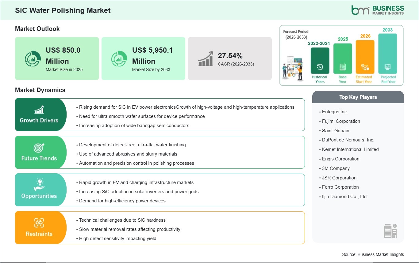
The SiC Wafer Polishing Market size is expected to reach US$ 5,950.1 million by 2033 from US$ 850. million in 2025. The market is estimated to record a CAGR of 27.54% from 2026 to 2033.
The global silicon carbide (SiC) wafer polishing market is a highly specialized segment within the semiconductor materials industry, driven by the increasing adoption of wide bandgap semiconductors in high-power and high-frequency applications. SiC wafers are critical for devices used in electric vehicles, renewable energy systems, industrial power electronics, and advanced telecommunications, where efficiency, thermal performance, and durability are essential. Polishing plays a crucial role in achieving defect-free, ultra-smooth wafer surfaces required for epitaxial layer growth and device fabrication. The market is gaining momentum due to the rapid expansion of electric mobility and energy-efficient power conversion technologies, which rely heavily on SiC-based components.
Additionally, the transition toward higher wafer diameters and improved device yields is increasing the demand for advanced chemical mechanical polishing (CMP) solutions tailored for SiC substrates. However, the market faces notable challenges, including the inherent hardness of SiC material, which makes polishing complex, time-consuming, and costly. The need for highly specialized slurries, pads, and equipment adds to operational expenses. Furthermore, achieving uniform surface quality without introducing subsurface damage remains a technical barrier, requiring continuous innovation and precision engineering in polishing processes.

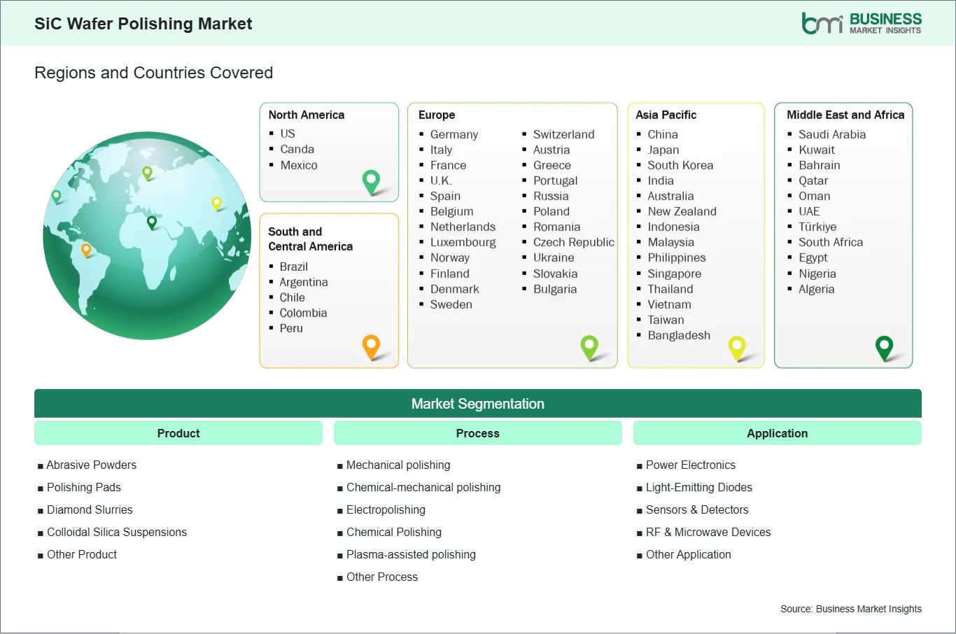
Key segments that contributed to the derivation of the SiC wafer polishing market analysis are product, process, and application
The Western Europe region for SiC wafer polishing is witnessing rapid growth due to the high demand for silicon carbide in electric vehicle power electronics. Germany and France are among the countries in Western Europe that are leading in the manufacture of electric vehicles. In these electric vehicles, silicon carbide is being widely used in power electronics such as inverters, on-board chargers, and power control units. For these power electronic devices, wafers need to have very smooth surfaces. Therefore, advanced wafer polishing techniques such as chemical mechanical polishing have become essential.
The automotive industry in Europe is focusing on achieving higher energy efficiency and driving range, both of which can be achieved through the utilization of SiC semiconductors, as they can operate at higher voltage and temperature. This has put more emphasis on achieving higher quality wafers, as even a slight imperfection on the surface of a wafer can impact the performance and lifespan of a semiconductor. Thus, polishing technologies are advancing to achieve higher precision, lower defect density, and uniformity on wafers, catering to the stringent quality of automotive-grade semiconductors.
Further, the presence of semiconductor fabrication and research facilities in countries such as the Netherlands and Italy has added to the scope of innovation in processing SiC wafers. This has led to a collaboration of automotive, semiconductor, and research companies to improve polishing slurries, pads, and equipment, thereby adding to Western Europe's ability to produce higher quality wafers, thus emphasizing the importance of polishing technologies in catering to the rising need for advanced EV power electronics.
The increased use of SiC devices in renewable energy systems and power grid infrastructure is another key driver for the SiC wafer polishing market in Western Europe. Countries such as Spain, Italy, and Germany are witnessing increased investments in solar energy systems, where SiC-based inverters are used due to their high efficiency and lower energy loss rates. These inverters demand high-quality SiC wafers with minimal surface defects, which are critical for their long-term usage and electrical properties.
Power grid modernization initiatives in Western Europe are also driving the demand for SiC devices. SiC devices are being integrated into the grid converters, smart distribution networks, and high-voltage transmission networks because they can operate under high power density conditions. Polished wafer surfaces with high surface integrity are required for these applications, as they can directly affect the performance and reliability of the SiC devices. As a result, there is a constant drive to improve the polishing processes to meet the requirements of the power grid applications.
In addition, the focus on sustainable and energy-efficient technologies in Western Europe is also driving the demand for high-performance semiconductor materials like SiC. Research initiatives and collaborations are being undertaken to improve the wafer processing techniques, including polishing, to reduce wafer defects. As the renewable energy and power grid infrastructure projects continue to grow in the region, the demand for precision polishing solutions is expected to increase, making Western Europe a promising market for SiC wafer processing technologies.

The global SiC wafer polishing market is experiencing steady growth, with market size and share analysis reflecting evolving treatment preferences and competitive dynamics among key players. The report evaluates important subsegments categorized within product, process, and application highlighting their respective contributions to overall market performance.
By product, the colloidal silica suspensions subsegment dominated the market in 2025 because it provides excellent surface planarity, low defectivity, and sub‑nanometer finish quality critical for high‑performance power devices. Unlike coarse abrasives or standard pads, colloidal silica’s chemical action enhances removal rates while minimizing scratches, making it the most adopted polishing media as SiC wafer quality demands increase.
By process, the chemical polishing segment subsegment dominated the market in 2025 because it offers the best balance of smoothness, throughput, and wafer integrity for SiC substrates used in power electronics. Pure mechanical methods struggle to deliver the tight surface finish required for high‑efficiency SiC devices, and purely chemical methods lack adequate material removal control. As device geometries shrink and performance expectations rise, CMP remains the primary method.
By application, the power electonics subsegment dominated the market in 2025 because of SiC’s superior efficiency, thermal performance, and breakdown voltage are increasingly critical in EVs, renewable energy, and industrial converters. These segments drive massive SiC wafer production and demand the highest surface quality — making power electronics the dominant end use for SiC wafer polishing materials and processes.
| Report Attribute | Details |
|---|---|
| Market size in 2025 | US$ 850.0 Million |
| Market Size by 2033 | US$ 5,950.1 Million |
| Global CAGR (2026 - 2033) | 27.54% |
| Historical Data | 2022-2024 |
| Forecast period | 2026-2033 |
| Segments Covered | By Product
|
|
Regions and Countries Covered
| |
| North America | US, Canada, Mexico |
| Europe | Belgium, Austria, Finland, Denmark, Greece, Poland, Romania, Russia, Ukraine, Czech Republic, Slovakia, Bulgaria, Italy, Luxembourg, Germany, Switzerland, France, Netherlands, Norway, Portugal, Spain, Sweden, United Kingdom |
| Asia-Pacific | Australia, China, India, Japan, South Korea, Indonesia, Malaysia, Philippines, Singapore, Thailand, Vietnam, Bangladesh, New Zealand, Taiwan |
| South and Central America | Brazil, Argentina, Peru, Chile, Colombia |
| Middle East and Africa | Bahrain, Kuwait, Oman, Qatar, Saudi Arabia, United Arab Emirates, Turkiye, South Africa, Egypt, Algeria, Nigeria |
| Market leaders and key company profiles |
|
The "SiC Wafer Polishing Market Size and Forecast (2022 - 2033)" report provides a detailed analysis of the market covering below areas:
The geographical scope of the SiC wafer polishing market report is divided into: North America, Asia Pacific, Europe, Middle East & Africa, and South & Central America. North America held the largest share in 2025.
North America leads the global SiC wafer polishing market, supported by a strong ecosystem of semiconductor innovation, advanced materials research, and power electronics development. The region is characterized by significant investments in next-generation semiconductor technologies, particularly in applications such as electric vehicles, aerospace systems, and renewable energy infrastructure, where SiC devices are increasingly preferred. The presence of leading research institutions and technology companies fosters continuous advancement in wafer polishing techniques, including the development of optimized CMP slurries and precision polishing equipment tailored for SiC substrates.
North America’s emphasis on domestic semiconductor manufacturing and supply chain independence further drives the demand for localized polishing capabilities, ensuring higher quality control and reduced reliance on external suppliers. Additionally, collaborations between equipment manufacturers, material suppliers, and semiconductor firms accelerate innovation in achieving defect-free wafer surfaces and improving production efficiency. Despite its leadership position, the region faces challenges related to high operational costs and the complexity of scaling polishing processes for larger wafer sizes. Environmental considerations and the need for sustainable polishing solutions also push companies to invest in eco-friendly consumables and waste reduction technologies, shaping the future trajectory of the market in North America.

The SiC wafer polishing market is evaluated by gathering qualitative and quantitative data post primary and secondary research, which includes important corporate publications, association data, and databases. A few of the key developments in the SiC wafer polishing market are:
The SiC Wafer Polishing Market is valued at US$ 850.0 Million in 2025, it is projected to reach US$ 5,950.1 Million by 2033.
As per our report SiC Wafer Polishing Market, the market size is valued at US$ 850.0 Million in 2025, projecting it to reach US$ 5,950.1 Million by 2033. This translates to a CAGR of approximately 27.54% during the forecast period.
The SiC Wafer Polishing Market report typically cover these key segments-
The historic period, base year, and forecast period can vary slightly depending on the specific market research report. However, for the SiC Wafer Polishing Market report:
The SiC Wafer Polishing Market is populated by several key players, each contributing to its growth and innovation. Some of the major players include:
The SiC Wafer Polishing Market report is valuable for diverse stakeholders, including:
Essentially, anyone involved in or considering involvement in the SiC Wafer Polishing Market value chain can benefit from the information contained in a comprehensive market report.
Please tell us your area of interest
(Market Segments/ Regions and Countries/ Companies)