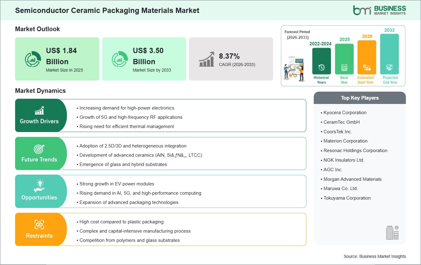
The Semiconductor Ceramic Packaging Materials Market size is expected to reach US$ 3.5 billion by 2033 from US$ 1.84 billion in 2025. The market is estimated to record a CAGR of 8.37% from 2026 to 2033.
Executive Summary and Global Market Analysis:
The global semiconductor ceramic packaging materials market is experiencing steady evolution, driven by the increasing complexity of electronic devices and the growing demand for high-performance, reliable semiconductor components. Ceramic materials such as alumina, aluminum nitride, and silicon nitride are widely preferred due to their superior thermal conductivity, electrical insulation, and mechanical strength, making them essential for advanced packaging applications in automotive electronics, telecommunications, aerospace, and high-power computing.
The rapid expansion of electric vehicles, 5G infrastructure, and artificial intelligence hardware is significantly influencing demand, as these applications require robust packaging solutions capable of withstanding high temperatures and harsh operating environments. Additionally, the shift toward miniaturization and higher integration densities is reinforcing the importance of ceramic packaging materials in ensuring device stability and longevity.
However, the market faces certain restraints, including the high cost of advanced ceramic materials and complex manufacturing processes, which can limit adoption among cost-sensitive manufacturers. Furthermore, competition from alternative packaging technologies, such as advanced polymers and organic substrates, presents a challenge, particularly in lower-performance applications where cost efficiency outweighs performance benefits.
Key segments that contributed to the derivation of the Semiconductor ceramic packaging materials market analysis are material, packaging technology and end use.
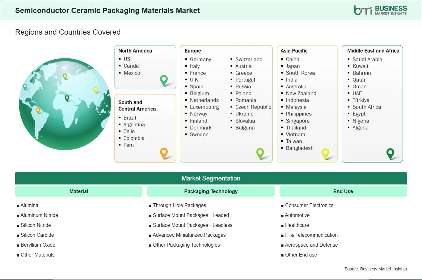
By material, the semiconductor ceramic packaging materials market is segmented into alumina, aluminum nitride, silicon nitride, silicon carbide, beryllium oxide, and other materials. The alumina segment dominated the market in 2025.
By packaging technology, the semiconductor ceramic packaging materials market is segmented into through-hole packages, surface mount packages - leaded, surface mount packages - leadless, advanced miniaturized packages, and other packaging technologies. The surface mount packages - leadless segment dominated the market in 2025.
In terms of end use, the semiconductor ceramic packaging materials market is segmented into consumer electronics, automotive, healthcare, it & telecommunication, aerospace and defense, and other end use. The automotive segment dominated the market in 2025.
Semiconductor Ceramic Packaging Materials Market Drivers and Opportunities:
Rising Demand for High-Power & High-Frequency Electronics
The Western Europe semiconductor ceramic packaging materials market is also influenced by the region's high focus on the electrification drive and industrial power electronics. The region's countries, such as Germany and France, are driving the electric vehicle market, as well as the industrial automation and renewable energy sectors. Ceramic substrates such as alumina and aluminium nitride are widely used in power modules due to their high voltage and heat resistance while still ensuring electrical insulation.
The increase in renewable energy systems, including solar and wind power systems, is another area that is increasing the scope for ceramic packaging materials. Power conversion systems in these types of applications require reliable performance in varying load conditions, and ceramic materials are preferred in these cases due to their capacity in managing heat and maintaining reliable performance.
High-frequency electronics in rail transport systems, aerospace, and industrial automation are another area of application for ceramic materials in packaging semiconductors. These types of applications include radar systems, signalling systems, and robotics, which require reliable performance in varying environmental conditions. Unlike consumer-oriented markets in regions like Asia, Western Europe is a highly reliable and high-value market segment, and ceramic materials are a strategic choice in these types of applications. The scope in industrial, transportation, and energy sectors ensures a steady growth rate in ceramic packaging materials in Western Europe and makes it a hub for high-end semiconductor applications.
5G, AI, and High-Performance Computing (HPC)
The move towards advanced digital infrastructure in Western Europe is fueling the adoption of ceramic packaging in semiconductors. The rollout of 5G infrastructure in countries like Sweden, Finland, and the UK is creating demand for RF modules and other high-frequency components. Ceramic substrates have low signal loss, thermal stability, and precision, making them suitable for base stations, small cells, and millimeter wave technologies.
Artificial intelligence and high-performance computing are creating opportunities for ceramic packages. Data centers in cities like Frankfurt, London, and Paris have high-power processors and multi-chip modules, which produce a lot of heat. Ceramic substrates provide efficient thermal management and reliable operation in these environments, which require stability in compute-intensive workloads.
Regional initiatives in advancing technological autonomy are another factor adding support to the regional market. Several research facilities and pilot manufacturing plants are currently in development to create ceramics used in AI accelerator packages, HPC systems, and other high-performance computing applications, particularly in terms of increased interconnect density and thermal performance. As such, ceramic packaging is a crucial element in advancing Western Europe’s digital and computing ecosystem, thus bolstering its importance as a region in support of next-generation semiconductor technology and associated electronics infrastructure.
Semiconductor Ceramic Packaging Materials Market Size and Share Analysis:
The global Semiconductor ceramic packaging materials market is experiencing steady growth, with market size and share analysis reflecting evolving treatment preferences and competitive dynamics among key players. The report evaluates important subsegments categorized within material, packaging technology and end use highlighting their respective contributions to overall market performance.
By material, the alumina subsegment dominated the market in 2025 due to its to its excellent cost‑to‑performance balance, high thermal conductivity, and strong electrical insulation. Its maturity in established processes and broad compatibility with multiple package types (e.g., DCB, thick film substrates) keeps it dominant as the industry transitions to higher power and reliability requirements.
By technology, the surface mount packages - leadless subsegment dominated the market in 2025 because they are well‑established, cost‑effective, and reliable for high‑power and high‑frequency applications like power modules and RF front‑ends. Despite growth in advanced miniaturized packages, many industrial and automotive applications still prioritize proven reliability and ease of assembly.
By end use, the automotive subsegment dominated the market in 2025 due to electrification, ADAS (Advanced Driver‑Assistance Systems), and EV power electronics. These vehicles require robust, thermally efficient ceramic packaging for inverters, sensors, and power modules — making automotive the fastest‑scaling and highest‑volume end use by 2025.
Australia, China, India, Japan, South Korea, Indonesia, Malaysia, Philippines, Singapore, Thailand, Vietnam, Bangladesh, New Zealand, Taiwan
South and Central America
Brazil, Argentina, Peru, Chile, Colombia
Middle East and Africa
Bahrain, Kuwait, Oman, Qatar, Saudi Arabia, United Arab Emirates, Turkiye, South Africa, Egypt, Algeria, Nigeria
Market leaders and key company profiles
Kyocera Corporation
CeramTec GmbH
CoorsTek Inc.
Materion Corporation
Resonac Holdings Corporation
NGK Insulators Ltd.
AGC Inc.
Morgan Advanced Materials
Maruwa Co. Ltd.
Tokuyama Corporation
Get more information on this report
Semiconductor Ceramic Packaging Materials Market Report Coverage and Deliverables:
The "Semiconductor Ceramic Packaging Materials Market Size and Forecast (2022 - 2033)" report provides a detailed analysis of the market covering below areas:
Semiconductor ceramic packaging materials market size and forecast at the regional and country levels for segments covered under the scope
Semiconductor ceramic packaging materials market trends, as well as drivers, restraints, and opportunities
Semiconductor ceramic packaging materials market analysis covering key trends, regional framework, major players, regulations, and recent developments
Industry landscape and competition analysis covering market concentration, heat map analysis, prominent players, and recent developments for the semiconductor ceramic packaging materials market.
Detailed company profiles, including SWOT analysis
The geographical scope of the Semiconductor ceramic packaging materials market report is divided into: North America, Asia Pacific, Europe, Middle East & Africa, and South & Central America. North America held the largest share in 2025.
North America stands out as the dominant region in the global semiconductor ceramic packaging materials market, primarily due to its strong technological ecosystem and early adoption of advanced semiconductor packaging solutions. The presence of leading semiconductor manufacturers, research institutions, and defense-related industries has fostered continuous innovation in ceramic packaging technologies.
The region benefits from high demand in sectors such as aerospace, defense, and high-performance computing, where reliability and thermal management are critical. Additionally, increasing investments in domestic semiconductor manufacturing and supply chain resilience are further strengthening the demand for advanced packaging materials. The push for localized production, particularly in response to global supply chain disruptions, is encouraging the development of high-quality ceramic substrates within the region. North America also leads in the adoption of next-generation technologies, including wide bandgap semiconductors, which require advanced ceramic packaging for optimal performance. Despite its dominance, the region faces challenges related to high production costs and environmental regulations, prompting manufacturers to focus on process optimization and sustainable material development.
Get more information on this report
Semiconductor Ceramic Packaging Materials Market Research Report Guidance:
The report includes qualitative and quantitative data in the semiconductor ceramic packaging materials market across material, packaging technology, end use, and geography.
The report starts with the key takeaways (chapter 2), highlighting the key trends and outlook of the Semiconductor ceramic packaging materials market.
Chapter 3 focuses on the research methodology of the study.
Chapter 4 includes ecosystem analysis.
Chapter 5 highlights the major industry dynamics in the semiconductor ceramic packaging materials market, including factors that are driving the market, prevailing deterrents, potential opportunities, as well as future trends. Impact analysis of these drivers and restraints is also covered in this section.
Chapter 6 discusses the Semiconductor ceramic packaging materials market scenario, in terms of historical market revenues, and forecast till the year 2033.
Chapters 7 to 10 cover the semiconductor ceramic packaging materials market segments by material, packaging technology, end use, and geography across North America, Europe, Asia Pacific, the Middle East and Africa, and South and Central America. They cover the market revenue, forecast, and factors driving the market.
Chapter 11 describes the competitive analysis along with the heat map analysis for the key players operating in the market.
Chapter 12 describes the industry landscape analysis. It provides detailed descriptions of business activities such as market initiatives, new developments, mergers, and joint ventures globally, along with a competitive landscape.
Chapter 13 provides detailed profiles of the major companies operating in the semiconductor ceramic packaging materials market. Companies have been profiled on the basis of their key facts, business descriptions, products, financial overview, SWOT analysis, and key developments.
Chapter 14, i.e., the appendix, is inclusive of a brief overview of the company, list of abbreviations, and disclaimer.
Semiconductor Ceramic Packaging Materials Market News and Key Development:
The semiconductor ceramic packaging materials market is evaluated by gathering qualitative and quantitative data post primary and secondary research, which includes important corporate publications, association data, and databases. A few of the key developments in the Semiconductor ceramic packaging materials market are:
In April 2025, Applied Materials, announced that it acquired a ~9% stake in BE Semiconductor Industries (BESI), a Netherlands-based advanced semiconductor packaging equipment company, to strengthen collaboration in hybrid bonding and advanced packaging technologies used across Europe, including Eastern European semiconductor supply chains.
In October 2024, multiple European semiconductor material suppliers, reported a strategic recovery plan and renewed investments in semiconductor packaging materials (including ceramic-based substrates) as the European market prepared for growth after a 2023 downturn, with increased focus on regional supply chain resilience and manufacturing activities across Central and Eastern Europe.
In 2023 (ongoing implementation phase), the European Union, advanced funding and policy support under its semiconductor strategy (linked to the European Chips Act), encouraging expansion of semiconductor materials and packaging ecosystems—including ceramic packaging materials—across member states in Eastern Europe to reduce dependency on Asia and strengthen local production capabilities.
Key Sources Referred:
EU REACH Regulation
European Chemicals Agency (ECHA)
Environmental Protection Agency (EPA)
Ministry of Economy Trade and Industry
Company Websites
Company Annual Reports
Company Investor Presentations
The List of Companies - Semiconductor Ceramic Packaging Materials Market
Kyocera Corporation
CeramTec GmbH
CoorsTek Inc.
Materion Corporation
Resonac Holdings Corporation
NGK Insulators Ltd.
AGC Inc.
Morgan Advanced Materials
Maruwa Co. Ltd.
Tokuyama Corporation
Frequently Asked Questions
How big is the Semiconductor Ceramic Packaging Materials Market?
The Semiconductor Ceramic Packaging Materials Market is valued at US$ 1.84 Billion in 2025, it is projected to reach US$ 3.50 Billion by 2033.
What is the CAGR for Semiconductor Ceramic Packaging Materials Market by (2026 - 2033)?
As per our report Semiconductor Ceramic Packaging Materials Market, the market size is valued at US$ 1.84 Billion in 2025, projecting it to reach US$ 3.50 Billion by 2033. This translates to a CAGR of approximately 8.37% during the forecast period.
What segments are covered in this report?
The Semiconductor Ceramic Packaging Materials Market report typically cover these key segments-
Material (Alumina, Aluminum Nitride, Silicon Nitride, Silicon Carbide, Beryllium Oxide, Other Materials)
Packaging Technology (Through-Hole Packages, Surface Mount Packages - Leaded, Surface Mount Packages - Leadless, Advanced Miniaturized Packages, Other Packaging Technologies)
End Use (Consumer Electronics, Automotive, Healthcare, IT & Telecommunication, Aerospace and Defense, Other End use)
What is the historic period, base year, and forecast period taken for Semiconductor Ceramic Packaging Materials Market?
The historic period, base year, and forecast period can vary slightly depending on the specific market research report. However, for the Semiconductor Ceramic Packaging Materials Market report:
Historic Period : 2022-2024
Base Year : 2025
Forecast Period : 2026-2033
Who are the major players in Semiconductor Ceramic Packaging Materials Market?
The Semiconductor Ceramic Packaging Materials Market is populated by several key players, each contributing to its growth and innovation. Some of the major players include:
Kyocera Corporation
CeramTec GmbH
CoorsTek Inc.
Materion Corporation
Resonac Holdings Corporation
NGK Insulators Ltd.
AGC Inc.
Morgan Advanced Materials
Maruwa Co. Ltd.
Tokuyama Corporation
Who should buy this report?
The Semiconductor Ceramic Packaging Materials Market report is valuable for diverse stakeholders, including:
Investors: Provides insights for investment decisions pertaining to market growth, companies, or industry insights. Helps assess market attractiveness and potential returns.
Industry Players: Offers competitive intelligence, market sizing, and trend analysis to inform strategic planning, product development, and sales strategies.
Suppliers and Manufacturers: Helps understand market demand for components, materials, and services related to concerned industry.
Researchers and Consultants: Provides data and analysis for academic research, consulting projects, and market studies.
Financial Institutions: Helps assess risks and opportunities associated with financing or investing in the concerned market.
Essentially, anyone involved in or considering involvement in the Semiconductor Ceramic Packaging Materials Market value chain can benefit from the information contained in a comprehensive market report.


 Get Free Sample For Semiconductor Ceramic Packaging Materials Market


