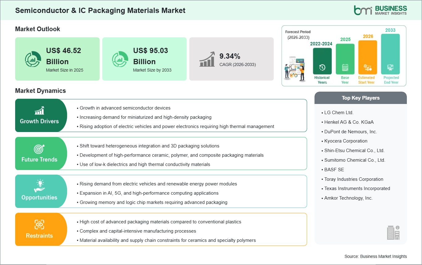
The Semiconductor & IC Packaging Materials Market size is expected to reach US$ 95.03 billion by 2033 from US$ 46.52 billion in 2025. The market is estimated to record a CAGR of 9.34% from 2026 to 2033.
Executive Summary and Global Market Analysis:
The global semiconductor and IC packaging materials market is a significant part of the semiconductor industry and provides the required solutions for the protection, interconnection, and improvement of the performance of semiconductor devices. The main driver of the market is the growing need for miniaturized and high-performance electronic devices in different fields such as consumer electronics, the automotive industry, telecommunications, and industrial sectors.
The use of high-performance packaging materials such as epoxy molding compounds, lead frames, substrates, and thermal interface materials is essential for ensuring the reliability of devices, especially for those that are miniaturized and operate at high frequencies. The development of new technologies such as 5G infrastructure, artificial intelligence devices, and electric vehicles is also driving the demand for packaging materials that are required for the protection and improvement of the performance of devices. However, the high cost of materials and the need for precise processing are also challenges faced by the market.
The development of alternative packaging materials such as fan-out wafer-level packaging and 3D IC packaging is also posing challenges for companies that are using traditional packaging materials for the production of IC devices.
Semiconductor & IC Packaging Materials Market - Strategic Insights:
Get more information on this report
Semiconductor & IC Packaging Materials Market Segmentation Analysis:
Key segments that contributed to the derivation of the semiconductor & IC packaging materials market analysis are type, packaging technology, and end use.
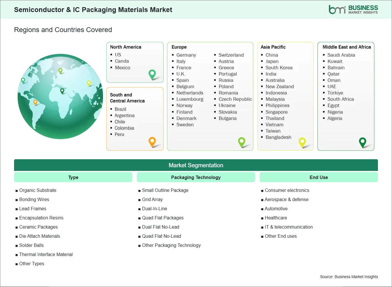
By type, the semiconductor & IC packaging materials market is segmented into organic substrate, bonding wires, lead frames, encapsulation resins, ceramic packages, die attach materials, solder balls, thermal interface material, and other types. The organic substrate segment dominated the market in 2025.
By Packaging technology, the semiconductor & IC packaging materials market is segmented small outline package, grid array, dual-in-line, quad flat packages, dual flat no-lead, quad flat no-lead, and other packaging technology. The grid array segment dominated the market in 2025.
In terms of end use, the semiconductor & IC packaging materials market is segmented into consumer electronics, aerospace & defense, automotive, healthcare, IT & telecommunication, others end use. The consumer electronic segment dominated the market in 2025.
Semiconductor & IC Packaging Materials Market Drivers and Opportunities:
Growth in Advanced Semiconductor Devices
The semiconductor IC packaging materials market in Western Europe is being driven by the advancements in technology in the development of new ICs such as artificial intelligence chips, high-performance computing ICs, and 5G ICs. The major technology centers in Germany, France, and the Netherlands are investing in the development of advanced chip technology. Chip technology development requires advanced IC packaging materials. Advanced IC packaging materials such as substrates, encapsulants, and thermal management materials play a vital role in managing the heat dissipation of these advanced ICs. Packaging techniques such as flip chip, wafer-level package, and 3D package are being used for the development of these advanced ICs.
The automotive and industrial electronics segments in Western Europe also contribute to the growth of the materials market. There has been an increased integration of AI chips in autonomous vehicles, industrial robots, and smart manufacturing equipment, which require IC packages that can withstand extreme temperatures, mechanical stress, and long lifespan. There is a strong need for thermal management materials and adhesives to support these applications. European countries require materials that not only perform well but also meet environmental and safety regulations, making locally sourced quality packaging materials strategically important.
The 5G infrastructure rollout in countries such as Sweden, Finland, and the UK also influences the growth of the IC packaging materials market. ICs in 5G base stations and communication devices require IC packages with low signal loss, thermal, and high-frequency performance. This trend also promotes the growth of specialty substrates and encapsulants for 5G IC packages, particularly those with high-frequency performance. Overall, the growth of AI, HPC, and 5G devices has strategically placed Western Europe as a significant contributor to the growth of IC packaging materials innovation.
Expansion in AI, 5G, and High-Performance Computing Applications
The growth of AI, 5G, and high-performance computing in Western Europe is one of the major growth drivers for semiconductor and IC packaging materials. Data centers in cities such as Frankfurt, Paris, and Amsterdam are growing to support cloud computing and AI workloads, which increases the demand for IC packages that provide reliable heat dissipation. Advanced IC packaging materials such as copper-molded substrates, high-performance solders, and thermal interface materials are used to enable high-density integration while ensuring system stability during operation.
In the telecommunication industry, the implementation of 5G technology is generating a strong demand for RF IC packages designed to operate at high frequencies without any significant loss in signal strength. Equipment makers in Europe place great importance on materials that offer high electrical performance and thermal reliability, as these parameters are critical in base stations, small cells, and mmWave modules. Packaging materials must also satisfy mechanical and environmental requirements in Europe, thus underlining the importance of materials.
AI and HPC-based applications in research, automotive, and industrial segments are another factor contributing to material demand. These applications require advanced materials in multi-chip modules, heterogeneous integration, and 3D stacked architectures, which can support high transistor density and high temperatures. The emphasis on regional innovation and technology self-sufficiency in Europe is fueling indigenous packaging materials, thus strengthening regional supply chains and enabling regional growth in AI, 5G, and HPC technology in Western Europe.
Semiconductor & IC Packaging Materials Market Size and Share Analysis:
The global semiconductor & IC packaging materials market is experiencing steady growth, with market size and share analysis reflecting evolving treatment preferences and competitive dynamics among key players. The report evaluates important subsegments categorized within type, packaging technology and end use highlighting their respective contributions to overall market performance.
By type, the organic substrate segment subsegment dominated the market in 2025 because they offer the best combination of cost‑efficiency, manufacturability, and high‑density interconnect capability for mainstream packaging. As advanced logic and memory packages scale (e.g., high‑performance BGAs and FC‑CSP), organic substrates remain preferred over more expensive ceramic or metal‑based types due to volume demand in mobile, computing, and consumer electronics.
By packaging technology, the grid array subsegment dominated the market in 2025 because they enable high I/O counts, improved electrical performance, and efficient heat dissipation, which are essential for modern ICs in computing, smartphones, and automotive electronics. Their wide adoption in both logic and memory keeps them ahead of conventional lead packages.
By end use, the consumer electronic subsegment dominated the market in 2025 because products like smartphones, tablets, wearables, and home devices still represent the largest volume of IC shipments worldwide. This high unit demand drives the largest absolute consumption of packaging materials even as other sectors (automotive, aerospace) grow rapidly on a percentage basis.
Semiconductor & IC Packaging Materials Market Report Highlights:
Australia, China, India, Japan, South Korea, Indonesia, Malaysia, Philippines, Singapore, Thailand, Vietnam, Bangladesh, New Zealand, Taiwan
South and Central America
Brazil, Argentina, Peru, Chile, Colombia
Middle East and Africa
Bahrain, Kuwait, Oman, Qatar, Saudi Arabia, United Arab Emirates, Turkiye, South Africa, Egypt, Algeria, Nigeria
Market leaders and key company profiles
LG Chem Ltd.
Henkel AG & Co. KGaA
DuPont de Nemours, Inc.
Kyocera Corporation
ShinâEtsu Chemical Co., Ltd.
Sumitomo Chemical Co., Ltd.
BASF SE
Toray Industries Corporation
Texas Instruments Incorporated
Amkor Technology, Inc.
Get more information on this report
Semiconductor & IC Packaging Materials Market Report Coverage and Deliverables:
The "Semiconductor & IC packaging materials market Size and Forecast (2022 - 2033)" report provides a detailed analysis of the market covering below areas:
Semiconductor & IC packaging materials market size and forecast at the regional and country levels for segments covered under the scope
Semiconductor & IC packaging materials market trends, as well as drivers, restraints, and opportunities
Semiconductor & IC packaging materials market analysis covering key trends, regional framework, major players, regulations, and recent developments
Industry landscape and competition analysis covering market concentration, heat map analysis, prominent players, and recent developments for the semiconductor & IC packaging materials market.
Detailed company profiles, including SWOT analysis
Semiconductor & IC Packaging Materials Market Geographic Insights:
The geographical scope of the Semiconductor & IC packaging materials market report is divided into: North America, Asia Pacific, Europe, Middle East & Africa, and South & Central America. North America held the largest share in 2025.
North America is the leading region in the semiconductor and IC packaging materials market, benefiting from a mature semiconductor ecosystem and strong technological infrastructure. The presence of major semiconductor manufacturers, advanced R&D centers, and high-performance computing industries drives the demand for innovative packaging materials capable of supporting complex device architectures.
The region is a pioneer in adopting advanced packaging techniques, such as system-in-package (SiP) and heterogeneous integration, which require sophisticated materials to maintain thermal management, mechanical stability, and electrical performance. Additionally, the push for domestic semiconductor production in North America is encouraging the development of localized, high-quality packaging materials to reduce supply chain dependency and enhance resilience. The growth of automotive electronics, aerospace applications, and defense systems further reinforces the market, as these sectors demand materials that can withstand rigorous operational conditions.
Despite its dominance, North America faces challenges from the high cost of materials and stringent environmental regulations, prompting manufacturers to focus on sustainability, process efficiency, and next-generation material innovation.
Get more information on this report
Semiconductor & IC Packaging Materials Market Research Report Guidance:
The report includes qualitative and quantitative data in the semiconductor & IC packaging materials market across type, packaging technology, end use, and geography.
The report starts with the key takeaways (chapter 2), highlighting the key trends and outlook of the Semiconductor & IC packaging materials market.
Chapter 3 focuses on the research methodology of the study.
Chapter 4 includes ecosystem analysis.
Chapter 5 highlights the major industry dynamics in the semiconductor & IC packaging materials market, including factors that are driving the market, prevailing deterrents, potential opportunities, as well as future trends. Impact analysis of these drivers and restraints is also covered in this section.
Chapter 6 discusses the Semiconductor & IC packaging materials market scenario, in terms of historical market revenues, and forecast till the year 2033.
Chapters 7 to 10 cover the semiconductor & IC packaging materials market segments by type, technology, end use, and geography across North America, Europe, Asia Pacific, the Middle East and Africa, and South and Central America. They cover the market revenue, forecast, and factors driving the market.
Chapter 11 describes the competitive analysis along with the heat map analysis for the key players operating in the market.
Chapter 12 describes the industry landscape analysis. It provides detailed descriptions of business activities such as market initiatives, new developments, mergers, and joint ventures globally, along with a competitive landscape.
Chapter 13 provides detailed profiles of the major companies operating in the semiconductor & IC packaging materials market. Companies have been profiled on the basis of their key facts, business descriptions, products, financial overview, SWOT analysis, and key developments.
Chapter 14, i.e., the appendix, is inclusive of a brief overview of the company, list of abbreviations, and disclaimer.
Semiconductor & IC Packaging Materials Market News and Key Development:
The semiconductor & IC packaging materials market is evaluated by gathering qualitative and quantitative data post primary and secondary research, which includes important corporate publications, association data, and databases. A few of the key developments in the Semiconductor & IC packaging materials market are:
In March 2026, SEMI Europe announced that it had signed a two‑year Memorandum of Understanding (MoU) with the Polish‑Taiwanese Chamber of Commerce to advance semiconductor industry expansion in Poland, aiming to support broader cooperation that could benefit semiconductor packaging materials supply chains and collaborations in Eastern Europe.
In April 2025, Applied Materials acquired approximately 9% stake in BE Semiconductor Industries (BESI), a Dutch advanced packaging tools and materials company, signaling strategic interest and potential collaboration that may influence the European packaging materials ecosystem including Eastern European supply chain roles.
In April 2024, Infineon Technologies AG announced that it had entered a multi‑year partnership with Amkor Technology, Inc., to operate a dedicated semiconductor packaging and test center at Amkor’s manufacturing site in Porto, Portugal, expanding advanced packaging capacity and strengthening the European IC packaging supply chain.
Key Sources Referred:
EU REACH Regulation
European Chemicals Agency (ECHA)
Packaging & Packaging Waste Regulation (PPWR)
Company Websites
Company Annual Reports
Company Investor Presentations
The List of Companies - Semiconductor & IC Packaging Materials Market
LG Chem Ltd.
Henkel AG & Co. KGaA
DuPont de Nemours, Inc.
Kyocera Corporation
Shin‑Etsu Chemical Co., Ltd.
Sumitomo Chemical Co., Ltd.
BASF SE
Toray Industries Corporation
Texas Instruments Incorporated
Amkor Technology, Inc.
Frequently Asked Questions
How big is the Semiconductor & IC Packaging Materials Market?
The Semiconductor & IC Packaging Materials Market is valued at US$ 46.52 Billion in 2025, it is projected to reach US$ 95.03 Billion by 2033.
What is the CAGR for Semiconductor & IC Packaging Materials Market by (2026 - 2033)?
As per our report Semiconductor & IC Packaging Materials Market, the market size is valued at US$ 46.52 Billion in 2025, projecting it to reach US$ 95.03 Billion by 2033. This translates to a CAGR of approximately 9.34% during the forecast period.
What segments are covered in this report?
The Semiconductor & IC Packaging Materials Market report typically cover these key segments-
Type (Organic Substrate, Bonding Wires, Lead Frames, Encapsulation Resins, Ceramic Packages, Die Attach Materials, Solder Balls, Thermal Interface Material, Other Types)
End Use (Consumer electronics, Aerospace & defense, Automotive, Healthcare, IT & telecommunication, Other End uses)
What is the historic period, base year, and forecast period taken for Semiconductor & IC Packaging Materials Market?
The historic period, base year, and forecast period can vary slightly depending on the specific market research report. However, for the Semiconductor & IC Packaging Materials Market report:
Historic Period : 2022-2024
Base Year : 2025
Forecast Period : 2026-2033
Who are the major players in Semiconductor & IC Packaging Materials Market?
The Semiconductor & IC Packaging Materials Market is populated by several key players, each contributing to its growth and innovation. Some of the major players include:
LG Chem Ltd.
Henkel AG & Co. KGaA
DuPont de Nemours, Inc.
Kyocera Corporation
ShinâÂÂEtsu Chemical Co., Ltd.
Sumitomo Chemical Co., Ltd.
BASF SE
Toray Industries Corporation
Texas Instruments Incorporated
Amkor Technology, Inc.
Who should buy this report?
The Semiconductor & IC Packaging Materials Market report is valuable for diverse stakeholders, including:
Investors: Provides insights for investment decisions pertaining to market growth, companies, or industry insights. Helps assess market attractiveness and potential returns.
Industry Players: Offers competitive intelligence, market sizing, and trend analysis to inform strategic planning, product development, and sales strategies.
Suppliers and Manufacturers: Helps understand market demand for components, materials, and services related to concerned industry.
Researchers and Consultants: Provides data and analysis for academic research, consulting projects, and market studies.
Financial Institutions: Helps assess risks and opportunities associated with financing or investing in the concerned market.
Essentially, anyone involved in or considering involvement in the Semiconductor & IC Packaging Materials Market value chain can benefit from the information contained in a comprehensive market report.


 Get Free Sample For Semiconductor & IC Packaging Materials Market


