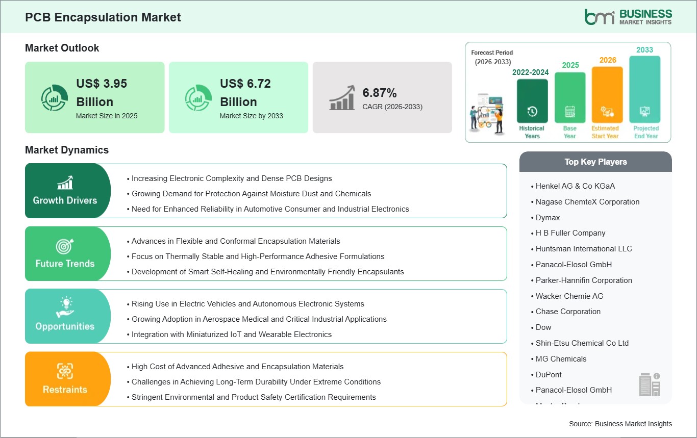
The PCB Encapsulation Market size is expected to reach US$ 6.72 billion by 2033 from US$ 3.95 billion in 2025. The market is estimated to record a CAGR of 6.87% from 2026 to 2033.
Executive Summary and Global Market Analysis:
The global market for PCB encapsulation plays a significant role in ensuring the reliability and durability of electronic devices in different industries. PCB encapsulation is a process of applying a protective coating to a printed circuit board to prevent damage from moisture, dust, chemicals, vibrations, and heat. With the development of modern electronic devices that are complex, compact, and high-performance-based, the requirement for encapsulation has seen a significant rise.
The driving forces for the global market for PCB encapsulation include the rapid development of electronic devices and technologies, the increasing use of smart devices in different industries, and the growing use of automation and electrification in industries such as the automotive sector, aerospace industry, industrial equipment, and electronic devices.
The development of new materials such as resins and hybrids for encapsulation has shown improvement in thermal conductivity, chemical resistance, and mechanical properties. However, high-performance encapsulation materials and methods may be complex and require specialized knowledge. Environmental issues may also be a problem for manufacturers, who have to strike a balance between material performance and environmentally friendly and sustainable practices.
The demand for PCB encapsulation is increasing due to the increasing use of electronic devices in daily life and critical systems, which makes encapsulation a key driver for the reliability of electronic devices and the development of new technologies.
PCB Encapsulation Market - Strategic Insights:
Get more information on this report
PCB Encapsulation Market Segmentation Analysis:
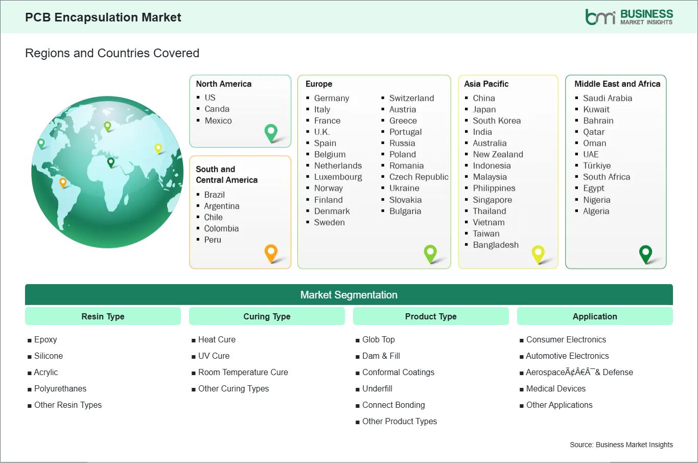
Key segments that contributed to the derivation of the PCB encapsulation market analysis are resin type, curing type, product type, and application.
By resin type, the PCB encapsulation market is segmented into epoxy, silicone, acrylic, polyurethanes, and other resin types. The epoxy subsegment dominated the market in 2025.
Based on curing type, the PCB encapsulation market is classified into heat cure, UV cure, room temperature cure, and other curing types. The UV cure subsegment dominated the market in 2025.
In terms of product type, the PCB encapsulation market is divided into glob top, dam & fill, conformal coatings, underfill, connect bonding, and other product types. The conformal coatings subsegment dominated the market in 2025.
On the basis of application, the PCB encapsulation market is categorized into consumer electronics, automotive electronics, aerospace & defense, medical devices, and other applications. The consumer electronics subsegment dominated the market in 2025.
PCB Encapsulation Market Drivers and Opportunities:
Increasing Electronic Complexity and Dense PCB Designs
The global PCB encapsulation market is strongly influenced by the rapid rise in electronic complexity and dense printed circuit board (PCB) designs. As electronic products become smaller and more powerful, PCB assemblies now often include extremely compact layouts, multilayer structures, embedded components, and miniaturized circuitry to meet performance targets while reducing footprint. These high‑density boards require advanced encapsulation techniques to provide robust physical protection, thermal management, and electrical insulation in environments where traditional conformal coatings may fall short. PCB encapsulation materials now must accommodate tighter component spacing, complex geometries, and higher component counts to prevent short circuits, moisture ingress, and mechanical stress.
In highly complex PCBs used in advanced electronic systems, the presence of microvias, blind vias, and higher‑layer counts increases the risk of dielectric breakdown and signal interference if protective materials are inadequate. As PCB designs push the limits of density to support high‑speed data transfer, multi‑layer boards, and embedded power semiconductors, encapsulation solutions are adapted to fill voids, absorb vibration, and strengthen solder joints. Modern encapsulants, like epoxies, polyurethanes, and silicones, provide thick protective layers that resist mechanical shock, moisture, and thermal cycling, ensuring reliability in demanding applications.
The push to densely integrate components has also accelerated the adoption of more sophisticated encapsulation techniques globally. Designers increasingly incorporate potting and overmolding into PCB manufacturing workflows to protect sensitive electronics against environmental threats, particularly in devices with long life expectations. Whether in industrial automation controls or high‑performance computing, encapsulation supports dense PCB architectures by enhancing reliability without compromising circuit integrity or adding excessive bulk.
Rising Use in Electric Vehicles and Autonomous Electronic Systems
The global PCB encapsulation market is also propelled by the rapid adoption of electric vehicles (EVs) and autonomous electronic systems, which depend heavily on high‑performance, reliable PCB assemblies. Modern EV powertrains, battery management units, inverters, and autonomous sensor arrays integrate sophisticated PCBs that must withstand harsh electrical, thermal, and mechanical operating conditions. Encapsulation becomes critical in these applications to ensure insulation at high voltages, stability under vibration, and moisture resistance for electronics that are subjected to wide temperature and humidity variations.
In autonomous electronic systems, such as advanced driver assistance or machine vision modules, sensor PCBs are tasked with processing vast amounts of data in real time. These boards are increasingly complex, featuring fine pitch components, high‑speed interconnects, and sensitive microelectronics. Encapsulation in such use cases serves not only to protect against environmental exposure but also to support thermal management and electromagnetic compatibility—reducing signal interference that could undermine real‑time processing and system accuracy.
As electric mobility and autonomous technologies mature across industries spanning from connected vehicles to robotics and industrial automation PCB encapsulation has transitioned from a protective option to a core engineering requirement. Encapsulation materials are selected not just for basic barrier protection but for performance under high electrical stress, thermal cycling, and continuous mechanical motion. This evolution underscores how rising integration of power electronics and autonomous functions directly shapes the demand for advanced encapsulation solutions that support durable, reliable electronic systems in real‑world applications.
PCB Encapsulation Market Size and Share Analysis:
The PCB encapsulation market is experiencing steady growth, with market size and share analysis reflecting evolving treatment preferences and competitive dynamics among key players. The report evaluates important subsegments categorized within resin type, curing type, product type, and application, highlighting their respective contributions to overall market performance.
By resin type, the Epoxy subsegment dominated the PCB Encapsulation market in 2025. Epoxy resins provide excellent mechanical strength, thermal stability, and chemical resistance, making them highly suitable for protecting sensitive electronic components, which drives their widespread adoption.
Based on curing type, the UV Cure subsegment dominated the PCB Encapsulation market in 2025. UV cure technologies offer rapid processing, energy efficiency, and precise application control, supporting strong demand for advanced PCB encapsulation solutions.
In terms of product type, the Conformal Coatings subsegment dominated the PCB Encapsulation market in 2025. Conformal coatings provide uniform protection against moisture, dust, and chemical exposure, enhancing the reliability and longevity of electronic assemblies, which reinforces the segment’s dominance.
On the basis of application, the Consumer Electronics subsegment dominated the PCB Encapsulation market in 2025. Consumer electronics require lightweight, durable, and highly reliable protection for circuit boards, driving strong adoption of PCB encapsulation materials in this sector.
Australia, China, India, Japan, South Korea, Indonesia, Malaysia, Philippines, Singapore, Thailand, Vietnam, Bangladesh, New Zealand, Taiwan
South and Central America
Brazil, Argentina, Peru, Chile, Colombia
Middle East and Africa
Bahrain, Kuwait, Oman, Qatar, Saudi Arabia, United Arab Emirates, Turkiye, South Africa, Egypt, Algeria, Nigeria
Market leaders and key company profiles
Henkel AG & Co KGaA
Nagase ChemteX Corporation
Dymax
H B Fuller Company
Huntsman International LLC
Panacol-Elosol GmbH
Parker-Hannifin Corporation
Wacker Chemie AG
Chase Corporation
Dow
Shin-Etsu Chemical Co Ltd
MG Chemicals
DuPont
Panacol-Elosol GmbH
Master Bond
Get more information on this report
PCB Encapsulation Market Report Coverage and Deliverables:
The "PCB Encapsulation Market Size and Forecast (2022 - 2033)" report provides a detailed analysis of the market covering below areas:
PCB Encapsulation market size and forecast at global, regional, and country levels for all the key market segments covered under the scope
PCB Encapsulation market trends, as well as drivers, restraints, and opportunities
PCB Encapsulation market analysis covering key trends, regional framework, major players, regulations, and recent developments
Industry landscape and competition analysis covering market concentration, heat map analysis, prominent players, and recent developments for the PCB Encapsulation market
Detailed company profiles, including SWOT analysis
PCB Encapsulation Market Geographic Insights:
The geographical scope of the PCB Encapsulation market report is divided into five regions: North America, Asia Pacific, Europe, Middle East & Africa, and South & Central America. The PCB Encapsulation market in North America is expected to grow during the forecast period.
North America is the leading region in PCB encapsulation due to its advanced electronics ecosystem, early adoption of innovative technologies, and presence of high-value industries. The region is home to a wide range of sectors that rely heavily on reliable electronics, including aerospace, automotive, medical devices, telecommunications, and industrial automation. These industries demand PCB protection solutions that can withstand harsh conditions such as vibration, high temperatures, humidity, and chemicals.
The focus for North American companies is on the development of encapsulation materials that not only withstand the above-mentioned conditions but also address the changing demands for the performance requirements of emerging technologies such as electric vehicles, smart infrastructure, and high-speed communication networks. Innovation is another important aspect where companies are focusing on the development of advanced resin materials, hybrid compounds, and coating technologies to enhance the performance requirements for PCB protection solutions.
The dominance of the North American region is also due to the strong association between companies, research institutions, and technology suppliers, which helps in the quick adoption of advanced PCB protection technologies. The challenges for the region include cost efficiency, high performance requirements, and environmental regulations. North America’s emphasis on technological innovation, quality, and sustainability continues to shape the global PCB encapsulation landscape and set benchmarks for other regions.
Get more information on this report
PCB Encapsulation Market Research Report Guidance:
The report includes qualitative and quantitative data in the PCB Encapsulation market across resin type, curing type, product type, application, and geography.
The report starts with the key takeaways (chapter 2), highlighting the key trends and outlook of the PCB Encapsulation market.
Chapter 3 focuses on the research methodology of the study.
Chapter 4 includes ecosystem analysis.
Chapter 5 highlights the major industry dynamics in the PCB Encapsulation market, including factors that are driving the market, prevailing deterrents, potential opportunities, as well as future trends. Impact analysis of these drivers and restraints is also covered in this section.
Chapter 6 discusses the PCB Encapsulation market scenario, in terms of historical market revenues, and forecast till the year 2033.
Chapters 7 to 11 cover the PCB Encapsulation market segments by resin type, curing type, product type, application, and geography across North America, Europe, Asia Pacific, Middle East and Africa, and South and Central America. They cover the market volume, revenue forecast, and factors driving the market.
Chapter 12 describes the competitive analysis with the heat map analysis for the key players operating in the market.
Chapter 13 describes the industry landscape analysis. It provides detailed descriptions of business activities such as market initiatives, new developments, mergers, and joint ventures globally, along with a competitive landscape.
Chapter 14 provides detailed profiles of the major companies operating in the PCB Encapsulation market. Companies have been profiled on the basis of their key facts, business descriptions, products, financial overview, SWOT analysis, and key developments.
Chapter 15, i.e., the appendix, is inclusive of a brief overview of the company, list of abbreviations, and disclaimer.
PCB Encapsulation Market News and Key Development:
The PCB encapsulation market is evaluated by gathering qualitative and quantitative data post primary and secondary research, which includes important corporate publications, association data, and databases. A few of the key developments in the PCB encapsulation market are:
In May 2024, H.B. Fuller Company announced the acquisition of ND Industries Inc., a U.S. specialty adhesives and fastener‑sealing solutions provider, expanding H.B. Fuller’s product portfolio including epoxy and UV curable materials used in electronics assembly and encapsulation and strengthening its global adhesives and coatings offerings used across automotive, aerospace, and electronics markets.
In February 2024, Henkel AG & Co. KGaA announced the commercialization of Loctite Stycast CC 8555, a new solvent‑free, UV‑curable conformal coating designed to provide high‑reliability protection for printed circuit boards (PCBs) and sensitive components in extreme environments, including industrial power electronics, EV charging infrastructure and high‑voltage systems.
Key Sources Referred:
International Organization for Standardization (ISO)American Society for Testing and Materials (ASTM International)Bureau of Indian Standards (BIS)Environmental Protection Agency (EPA), USAEuropean Chemicals Agency (ECHA)Central Pollution Control Board (CPCB), IndiaMinistry of Chemicals and Fertilizers, IndiaAmerican Chemistry Council (ACC)Indian Chemical Council (ICC)European Chemical Industry Council (Cefic)Specialty Chemical Association of India (SCAI)Company WebsitesCompany Annual ReportsCompany Investor Presentations
The List of Companies - PCB Encapsulation Market
Henkel AG & Co KGaA
Nagase ChemteX Corporation
Dymax
H B Fuller Company
Huntsman International LLC
Panacol-Elosol GmbH
Parker-Hannifin Corporation
Wacker Chemie AG
Chase Corporation
Dow
Shin-Etsu Chemical Co Ltd
MG Chemicals
DuPont
Panacol-Elosol GmbH
Master Bond
Frequently Asked Questions
How big is the PCB Encapsulation Market?
The PCB Encapsulation Market is valued at US$ 3.95 Billion in 2025, it is projected to reach US$ 6.72 Billion by 2033.
What is the CAGR for PCB Encapsulation Market by (2026 - 2033)?
As per our report PCB Encapsulation Market, the market size is valued at US$ 3.95 Billion in 2025, projecting it to reach US$ 6.72 Billion by 2033. This translates to a CAGR of approximately 6.87% during the forecast period.
What segments are covered in this report?
The PCB Encapsulation Market report typically cover these key segments-
Resin Type (Epoxy, Silicone, Acrylic, Polyurethanes, Other Resin Types)
Curing Type (Heat Cure, UV Cure, Room Temperature Cure, Other Curing Types)
Product Type (Glob Top, Dam & Fill, Conformal Coatings, Underfill, Connect Bonding, Other Product Types)
Application (Consumer Electronics, Automotive Electronics, Aerospaceâ¯& Defense, Medical Devices, Other Applications)
What is the historic period, base year, and forecast period taken for PCB Encapsulation Market?
The historic period, base year, and forecast period can vary slightly depending on the specific market research report. However, for the PCB Encapsulation Market report:
Historic Period : 2022-2024
Base Year : 2025
Forecast Period : 2026-2033
Who are the major players in PCB Encapsulation Market?
The PCB Encapsulation Market is populated by several key players, each contributing to its growth and innovation. Some of the major players include:
Henkel AG & Co KGaA
Nagase ChemteX Corporation
Dymax
H B Fuller Company
Huntsman International LLC
Panacol-Elosol GmbH
Parker-Hannifin Corporation
Wacker Chemie AG
Chase Corporation
Dow
Shin-Etsu Chemical Co Ltd
MG Chemicals
DuPont
Panacol-Elosol GmbH
Master Bond
Who should buy this report?
The PCB Encapsulation Market report is valuable for diverse stakeholders, including:
Investors: Provides insights for investment decisions pertaining to market growth, companies, or industry insights. Helps assess market attractiveness and potential returns.
Industry Players: Offers competitive intelligence, market sizing, and trend analysis to inform strategic planning, product development, and sales strategies.
Suppliers and Manufacturers: Helps understand market demand for components, materials, and services related to concerned industry.
Researchers and Consultants: Provides data and analysis for academic research, consulting projects, and market studies.
Financial Institutions: Helps assess risks and opportunities associated with financing or investing in the concerned market.
Essentially, anyone involved in or considering involvement in the PCB Encapsulation Market value chain can benefit from the information contained in a comprehensive market report.


 Get Free Sample For PCB Encapsulation Market


