
Lithography Equipment Market Outlook: Size, Share, Trends, Growth Analysis, Competitive Landscape & Forecast, 2026-2033

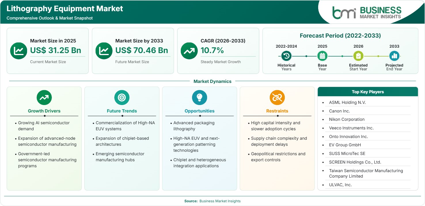
The Lithography Equipment Market size was valued at US$ 31.25 Billion in 2025 and is projected to reach US$ 70.46 Billion by 2033, growing at a CAGR of 10.7% during 2026–2033. Demand is supported by AI semiconductor fabrication, advanced node migration, heterogeneous integration, advanced packaging adoption, and rising capital expenditure across foundries, memory manufacturers, and integrated device manufacturers.

Report Coverage
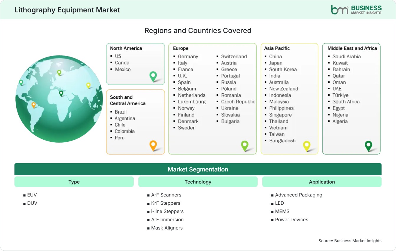
  • Type: EUV, DUV
  • Technology: ArF Scanners, KrF Steppers, i-line Steppers, ArF Immersion, Mask Aligners
  • Application: Advanced Packaging, LED, MEMS, Power Devices
US$ 31.25 Bn Market size in 2025
US$ 70.46 Bn Market Size by 2033
10.7% CAGR, 2026 - 2033
2026-2033 Forecast Period

AI Overview

Lithography Equipment Market Summary

  • North America Region: Holds 24%–27% share in 2025, growing at 9.5%–10.5% CAGR during 2026–2033. Key drivers include semiconductor reshoring, CHIPS Act funding, AI processor demand, and advanced packaging investments. The U.S. market benefits from domestic fab expansion and is projected to grow at 9.8%–10.8% CAGR.
  • Fastest Growing Region: Asia Pacific accounts for 42%–46% share in 2025 and expands at 11.8%–12.8% CAGR. Growth is supported by foundry investments, government incentives, packaging ecosystem expansion, and increasing local semiconductor manufacturing capacity.
  • Leading Segment: DUV holds 68%–72% share in 2025 and grows at 8.8%–9.8% CAGR. Demand remains strong across mature-node production, automotive semiconductors, industrial electronics, and power device manufacturing globally.
  • High Growth Segment: EUV represents 28%–32% share in 2025 and advances at 14.5%–15.5% CAGR. Adoption accelerates through sub-7nm production, AI accelerators, high-performance computing processors, and advanced memory fabrication requirements.
  • Key Market Opportunity: Expansion of advanced packaging platforms including 3D IC, 2.5D interposers, and wafer-level packaging creates substantial demand for next-generation lithography tools supporting heterogeneous integration and AI-centric semiconductor architectures.
  • Major Market Players: ASML Holding N.V., Canon Inc., Nikon Corporation, Veeco Instruments Inc., Onto Innovation Inc., EV Group GmbH, SUSS MicroTec SE, SCREEN Holdings Co., Ltd., Taiwan Semiconductor Manufacturing Company Limited (packaging lithography ecosystem), and ULVAC, Inc.
Strategic Insights

Lithography Equipment Market: Strategic Insights

Lithography Equipment Market Strategic Framework
FREE PDF
Request your free sample
Request free sample
Stakeholder View

Key Takeaways

  • The value chain remains highly concentrated, with EUV capability centered among a limited number of suppliers while optics, light sources, masks, and metrology systems form critical dependencies.
  • Advanced packaging applications offer the strongest upside because AI processors increasingly rely on chiplets, high-bandwidth memory integration, and heterogeneous architectures.
  • Innovation is shifting toward High-NA EUV, maskless lithography, improved throughput, and tighter overlay control to support next-generation semiconductor geometries.
  • Asia Pacific presents the most compelling investment case due to fab construction pipelines, packaging infrastructure growth, and strong government support mechanisms.
  • Strategic partnerships and technology alliances continue to increase as suppliers seek integrated patterning, inspection, and packaging capabilities.
  • Sustainability initiatives are encouraging energy-efficient lithography systems that reduce resource consumption while maintaining productivity requirements.
Geographic Outlook

Lithography Equipment Market Regional Highlights

North America Lithography Equipment Market

North America accounted for 24%–27% of the Lithography Equipment Market share in 2025 and is projected to expand at 9.5%–10.5% CAGR through 2033. The region benefits from semiconductor manufacturing incentives, AI infrastructure demand, and strong research capabilities. Investments by leading foundries and integrated device manufacturers support equipment procurement. Packaging innovation, federal funding programs, and growing domestic production initiatives strengthen regional competitiveness across advanced semiconductor manufacturing activities.

  • U.S.-based fab construction expands demand for advanced patterning systems across logic, memory, and packaging facilities.
  • AI accelerator production increases equipment utilization and supports sustained capital expenditure planning.
  • Government-backed semiconductor resiliency programs improve domestic manufacturing competitiveness.
  • Research institutions accelerate commercialization of next-generation lithography technologies.

US Lithography Equipment Market

The United States represents 78%–82% of North American demand and is anticipated to grow at 9.8%–10.8% CAGR. Expanding domestic semiconductor production, advanced-node investments, and packaging technology development support equipment procurement. Major chip manufacturers continue capacity additions while government incentives encourage strategic supply-chain localization. Strong research ecosystems and collaboration between industry and academia support innovation and equipment deployment.

  • CHIPS-related investments support fabrication, packaging, and research infrastructure expansion.
  • AI processor manufacturing generates sustained demand for advanced lithography platforms.
  • Defense and high-performance computing requirements encourage domestic semiconductor production.
  • Technology partnerships accelerate adoption of emerging patterning solutions.

Europe Lithography Equipment Market

Europe held a 19%–22% share in 2025 and is forecast to achieve 9.2%–10.2% CAGR. The region benefits from semiconductor sovereignty initiatives, automotive semiconductor demand, and strong equipment manufacturing capabilities. Germany remains the leading market, while Ireland and Italy demonstrate accelerated investment momentum. Research collaborations and industrial digitization efforts support equipment deployment. Strong positioning in semiconductor equipment ecosystems enhances long-term competitiveness.

  • Germany leads regional demand with established semiconductor manufacturing infrastructure.
  • Ireland records among the fastest expansion rates due to fabrication investments.
  • Automotive electrification increases demand for power-device production capacity.
  • European Chips Act initiatives encourage technology and manufacturing investments.

Asia Pacific Lithography Equipment Market

Asia Pacific captured 42%–46% share in 2025 and records the fastest CAGR of 11.8%–12.8% through 2033. The region dominates semiconductor fabrication capacity, foundry activity, and advanced packaging investments. Taiwan, South Korea, Japan, and China remain major demand centers, while India emerges as a high-growth destination. Strong electronics manufacturing ecosystems and capital expenditure pipelines underpin regional leadership and continued Lithography Equipment Market growth.

  • Taiwan leads advanced foundry investments and leading-edge node production.
  • South Korea strengthens memory and packaging-related equipment demand.
  • China continues expanding mature-node and specialty semiconductor manufacturing capacity.
  • India records among the highest growth rates from a smaller base.
  • Advanced packaging investments support next-wave procurement activity.

Rest of World Lithography Equipment Market

Rest of World accounts for 8%–11% share and advances at 8.0%–9.0% CAGR. South and Central America are gradually increasing semiconductor-related investments focused on electronics manufacturing. In the Middle East and Africa, technology diversification programs and industrial development initiatives create niche opportunities. Israel remains a significant innovation center, while the UAE and Saudi Arabia are pursuing semiconductor ecosystem development.

  • Israel supports advanced semiconductor research and innovation programs.
  • UAE technology diversification strategies encourage electronics investments.
  • Saudi Arabia expands industrial technology capabilities through strategic initiatives.
  • Brazil remains a leading South American electronics manufacturing hub.
  • Regional governments increasingly target semiconductor ecosystem participation.
Global Market Geography
FREE PDF
Request your free sample
Request free sample
Segment Analysis

Lithography Equipment Market Segmentation

Type

Type segmentation is led by DUV technologies with 68%–72% share in 2025 and 8.8%–9.8% CAGR. EUV adoption expands rapidly with demand from advanced logic and memory manufacturing. The Lithography Equipment Market scope continues to widen as both mature-node and leading-edge semiconductor production require distinct lithography platforms.

  • EUV: Essential for advanced-node patterning supporting AI processors, HPC devices, and next-generation memory production.
  • DUV: Maintains strong relevance across automotive, industrial, analog, and power semiconductor manufacturing applications.

Technology

Technology adoption reflects varying semiconductor production needs. ArF immersion systems dominate advanced-volume manufacturing, while KrF and i-line solutions remain relevant for specialized applications. Overall segment growth reflects increasing process complexity and packaging innovation.

  • ArF Scanners: Widely used for advanced patterning requiring high throughput and precision performance.
  • KrF Steppers: Support mature-node manufacturing with cost-efficient production economics.
  • i-line Steppers: Remain important for MEMS, sensors, and specialty semiconductor fabrication.
  • ArF Immersion: Enables tighter geometries and higher transistor densities for advanced chips.
  • Mask Aligners: Commonly deployed in research, MEMS, and packaging-related processes.

Applications

Applications are evolving as packaging-driven semiconductor designs become increasingly relevant. Advanced packaging is driving industry growth due to the growing demand for artificial intelligence and high-performance computing systems. Lithography Equipment Market trends suggest a growing need for tools across front-end and back-end processing.

  • Advanced Packaging: Benefits from chiplet architectures and heterogeneous integration requirements.
  • LED: Demand supported by display technologies, automotive lighting, and specialty applications.
  • MEMS: Growth driven by sensors, industrial automation, and consumer electronics integration.
  • Power Devices: Increasing deployment in EVs, renewable energy systems, and industrial equipment.

Packaging Platforms

Packaging platforms have become strategically significant since the scalability of performance relies heavily on integration technologies. Investment is being made in 3D IC and 2.5D interposer solutions, while wafer-level packaging is making progress in consumer and AI devices.

  • 3D IC: Enables high-density integration and performance optimization for advanced computing.
  • 2.5D Interposer: Supports high-bandwidth interconnect architectures and chiplet deployment.
  • Wafer Level Chip Scale Packaging: Offers compact form factors and manufacturing efficiency.
  • FO WLP Wafer: Increasingly used in mobile devices and high-performance applications.
  • 3D WLP: Supports advanced heterogeneous integration and future packaging roadmaps.
Market Forces

Lithography Equipment Market Dynamics

Key Market Drivers

AI Infrastructure and Advanced Semiconductor Demand

Growing adoption of generative AI infrastructure is driving a sharp rise in demand for advanced chips, necessitating more complex patterning processes. Foundries are consistently scaling up their leading-edge capabilities to support the needs of accelerators, networks, and memories. AI servers use many more semiconductor components than regular computers; therefore, they have a consistent equipment purchase cycle. The trend toward smaller process nodes results in increased equipment utilization per wafer. Therefore, companies are making investments in advanced lithography equipment. This structural transition remains a fundamental contributor to industry expansion and long-term technology investment.

Growth of Advanced Packaging Ecosystems

Advanced packaging technology has become an essential enabler of semiconductor performance and innovation. With the ever-increasing difficulty and cost of transistor scaling, chiplet and heterogeneous integration have been adopted by companies to improve functionality and efficiency. Chiplet and heterogeneous integration require very accurate lithography solutions to perform redistribution layer, interposer, and wafer-level packaging processes. The increasing demand for AI processors, high-bandwidth memory, and complex computing systems is also driving investment in equipment. Hence, there are procurement opportunities available through advanced packaging technology.

Government-Led Semiconductor Manufacturing Programs

Government-led semiconductor manufacturing initiatives have played an important role in increasing global chip manufacturing capacity. Various national plans implemented in the United States, Europe, China, India, South Korea, and Japan have made substantial investments in fabrication plants, semiconductor packaging operations, and semiconductor research and development. Initiatives to provide government funding, subsidies, and tax benefits aid in decreasing the risk involved in financing the project and speeding up the execution process. They also contribute to localizing the supply chain, improving manufacturing capabilities within the nation, and enhancing resilience to any disruptions. With the commissioning of various manufacturing plants, there is increased demand for semiconductor equipment.

Key Market Opportunities

Commercialization of High-NA EUV Systems

The development of high-NA EUV platforms is a promising area of growth for the semiconductor industry, driven by the increasing complexity of process nodes pursued by manufacturers. Due to their superior resolution, they enable the production of smaller, more efficient, and power-saving chips without resorting to multi-patterning solutions. This contributes to increased efficiency of the manufacturing process, its yield, and cost-effectiveness. Equipment vendors that can deliver productivity and reliability improvements, along with lower operating costs, have everything to gain from the high demand for their products among leading foundries and memory producers. As a result, long-term lithography equipment market forecasts increasingly factor in the adoption of High-NA EUV and related ecosystem investments.

Expansion of Chiplet-Based Architectures

Chiplet-based architectures are gaining rapid adoption across artificial intelligence, networking, and high-performance computing applications due to their ability to improve performance, scalability, and cost efficiency. These designs depend on advanced semiconductor packaging technologies that require highly precise lithography processes. As chip integration becomes more complex, demand is increasing for systems capable of supporting redistribution layers, through-silicon connections, and sophisticated 3D packaging structures. Equipment suppliers with strong positions in advanced packaging workflows are expected to benefit significantly from the continued expansion of chiplet adoption across multiple end markets.

Emerging Semiconductor Hubs

The rise of new semiconductor manufacturing clusters in India, Southeast Asia, and certain Middle Eastern nations presents significant opportunities for growth in the global semiconductor equipment market. Huge investments in fabrication plants, assembly, testing, and advanced packaging facilities are boosting demand for manufacturing equipment and technology. The government is backing ecosystem building by providing various incentives, infrastructure spending, and industrial policies to attract semiconductor manufacturers. As regional ecosystems develop and manufacturing capabilities expand, demand for equipment is expected to grow steadily, creating long-term opportunities for market penetration and revenue growth for global suppliers.

Market Restraints and Challenges

High Capital Intensity and Slower Adoption Cycles

Lithography systems are among the most costly assets in a semiconductor fabrication plant. High purchase and operational costs. The procurement process is largely influenced by market demand visibility and financing considerations. Small-scale companies often face difficulties upgrading their technology, leading to longer equipment lifecycles. Economic volatility may delay the capital expenditure program, negatively affecting short-term equipment demand. These financial barriers remain a key challenge despite strong long-term growth fundamentals.

Supply Chain Complexity and Deployment Delays

State-of-the-art lithography systems require specialized optics, precise engineering, and high-precision parts. Factor: Limited supplier base and technical complexity. Downtime may cause delays in deliveries and installations and increase manufacturing expenses. Geopolitical constraints, export limitations, and parts availability further compound the uncertainties. Proper management of such dependencies is crucial for reliable equipment delivery schedules and continued operations.

Company Analysis

Competitive Landscape

The competitive environment remains concentrated around advanced patterning technologies. This Lithography Equipment Market analysis highlights leading participants across semiconductor manufacturing and packaging ecosystems.

Company Name

Overview

Products and Services relevant to this market

ASML Holding N.V.

Global leader in semiconductor lithography with dominant EUV and strong DUV portfolio.

EUV systems, DUV scanners, High-NA platforms, lithography software and productivity solutions.

Canon Inc.

Major provider of semiconductor and nanoimprint lithography technologies.

i-line steppers, nanoimprint lithography systems, semiconductor manufacturing equipment.

Nikon Corporation

Established supplier serving semiconductor and advanced packaging markets.

ArF immersion systems, steppers, digital lithography solutions, packaging tools.

Veeco Instruments Inc.

Semiconductor process equipment specialist with packaging exposure.

Lithography-related process solutions, advanced packaging manufacturing technologies.

Onto Innovation Inc.

Provides process control and packaging-enabling technologies.

Packaging inspection, metrology, lithography workflow optimization solutions.

EV Group GmbH

Leading advanced packaging and wafer bonding technology provider.

Lithography aligners, wafer bonding systems, heterogeneous integration solutions.

SUSS MicroTec SE

Established provider of lithography and semiconductor process tools.

Mask aligners, coating systems, advanced packaging lithography equipment.

SCREEN Holdings Co., Ltd.

Semiconductor manufacturing equipment supplier serving global fabs.

Wafer processing, coating, patterning-support technologies.

Taiwan Semiconductor Manufacturing Company Limited

Key ecosystem participant driving demand and process innovation.

Advanced manufacturing, packaging integration, technology development activities.

ULVAC, Inc.

Semiconductor equipment supplier supporting fabrication processes.

Vacuum process equipment and semiconductor manufacturing solutions.

Trust & Transparency

Research Methodology

The market analysis combines proprietary research with secondary data from government agencies, company disclosures, regulatory filings, industry databases and expert interviews. Market estimates are validated through data triangulation, cross-market benchmarking and analyst review.

View Full Research Methodology

Questions Answered

Frequently Asked Questions

What does the Lithography Equipment Market Report focus on?

The report evaluates market size, technology evolution, regional opportunities, competitive positioning, packaging developments, and strategic growth factors shaping future industry performance.

How does EUV differ from DUV technology?

EUV enables advanced-node manufacturing at smaller geometries, while DUV remains essential for mature-node, automotive, industrial, and specialty semiconductor production.

Which region dominates industry demand?

Asia Pacific leads global demand because it concentrates foundries, memory manufacturers, electronics production capacity, and semiconductor packaging ecosystems.

What application area offers the highest long-term opportunity?

Advanced packaging represents one of the strongest opportunities due to growing deployment of chiplets, 3D integration, and high-bandwidth memory architectures.

What factors are driving demand for advanced lithography solutions?

AI processors, advanced memory, semiconductor localization programs, and adoption of heterogeneous integration are increasing requirements for precision patterning technologies.

Access the Full Lithography Equipment Market Report

Get segment-level forecasts, regional estimates, competitive benchmarking, company profiles and downloadable Excel datasets.

Access the full Lithography Equipment Market Report
350 pages PDF & Excel | 2026-08-31