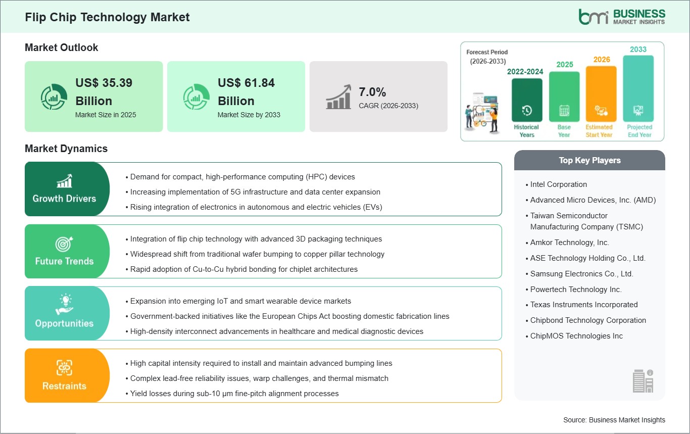
The Flip Chip Technology market size is expected to reach US$ 45.48 billion by 2033 from US$ 29.86 billion in 2025. The market is estimated to record a CAGR of 5.4% from 2026 to 2033.
Executive Summary and Global Market Analysis:
Flip chip technology refers to the integrated application of advanced semiconductor packaging solutions engineered to provide high-density electrical interconnections between an integrated circuit (IC) and its substrate. By utilizing a face-down assembly process where conductive bumps, primarily copper pillars or solder spheres, are placed directly on the chip surface and then flipped to bond with the package, these systems facilitate superior electrical and thermal performance compared to traditional wire bonding. This technology is fundamental to the operational architecture of high-performance computing (HPC) centers, next-generation 5G telecommunications, and advanced automotive electronics. Market expansion is being propelled by the rapid global transition toward miniaturized electronic devices, the rising institutional requirement for efficient heat dissipation in AI accelerators, and the increasing integration of Internet of Things (IoT) sensors that demand ultra-compact footprints.
However, several factors may restrain market progression. The high capital intensity associated with establishing advanced bumping lines, encompassing sophisticated lithography and plating equipment, remains a primary hurdle for outsourced semiconductor assembly and test (OSAT) providers. The industry also faces persistent technical challenges regarding wafer warpage and thermal stress, where the mismatch in thermal expansion coefficients between the silicon die and the organic substrate can lead to interconnect failure during the reflow process. Additionally, the proliferation of ultra-fine pitch requirements has intensified concerns regarding alignment accuracy and yield losses, as sub-10 µm spacing necessitates extremely precise thermocompression bonding (TCB) techniques. These hurdles, compounded by global semiconductor supply chain volatility and stringent environmental regulations regarding lead-free solder transitions, increase the total cost of ownership and may lengthen the development cycles for mid-range consumer electronic applications.
Despite these hurdles, the market outlook remains highly favorable as the sector transitions toward heterogeneous integration and 3D stacking. Opportunities are emerging through the adoption of Copper Pillar Bumping; the market is witnessing a surge in this technology due to its superior electromigration resistance and higher current-carrying capacity for high-end CPUs and GPUs. The automotive segment is gaining significant traction, with a rising requirement for flip chip packaging in Electric Vehicle (EV) engine control units and Advanced Driver Assistance Systems (ADAS) to ensure reliability in harsh thermal environments. Furthermore, the growth of Hybrid Bonding, which eliminates traditional bumps for direct copper-to-copper connections, aligns with global goals for achieving exascale computing speeds with minimal latency.
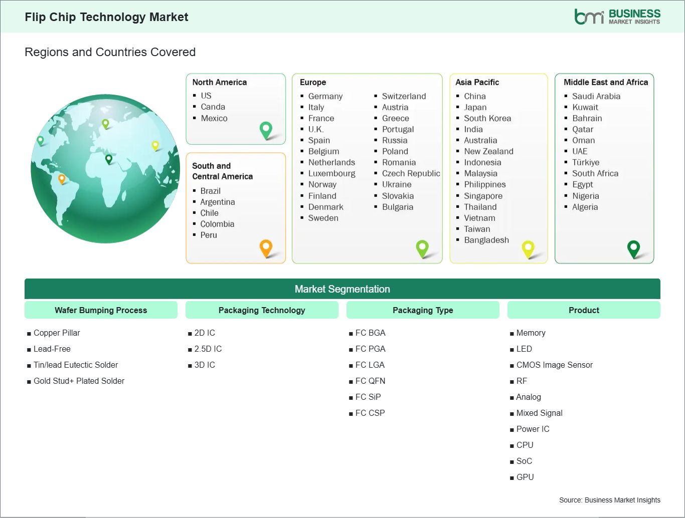
Key segments that contributed to the derivation of the Flip Chip Technology market analysis are wafer bumping process, packaging technology, packaging type, and product.
By Wafer Bumping Process, the market is segmented into Copper Pillar, Lead-Free, Tin/lead Eutectic Solder, and Gold Stud+ Plated Solder.
By Packaging Technology, the market is divided into 2D IC, 2.5D IC, and 3D IC.
By Packaging Type, the market is categorized into FC BGA, FC PGA, FC LGA, FC QFN, FC SiP, and FC CSP.
By Product, the market is segmented into Memory, LED, CMOS Image Sensor, RF, Analog, Mixed Signal, Power IC, CPU, SoC, and GPU.
Flip Chip Technology Market Drivers and Opportunities:
Rising Demand for Miniaturization, High‑Performance, and Reliability
The flip chip technology market is being driven by the growing need for miniaturization, high‑performance computing, and reliability across consumer electronics, automotive, telecommunications, and industrial sectors. Flip chip packaging allows direct electrical connection of semiconductor die to substrates, enabling higher input/output density, improved thermal performance, and reduced signal loss compared to traditional wire bonding. The rapid expansion of smartphones, tablets, and wearables is amplifying adoption, as manufacturers seek compact, energy‑efficient solutions that support advanced functionality. Automotive applications, including electric vehicles, ADAS, and infotainment systems, are reinforcing demand for robust flip chip designs that withstand harsh operating conditions. Data centers and cloud computing are also fueling growth, with flip chip technology supporting high‑speed processors and GPUs essential for AI, machine learning, and big data analytics. Additionally, stricter regulatory standards for reliability and performance are propelling investment in advanced packaging solutions. Collectively, miniaturization trends, performance requirements, and reliability priorities are fueling sustained growth in the global flip chip technology market.
Rising Integration of AI, IoT, and Emerging Applications
Opportunities in the flip chip technology market are expanding through the integration of artificial intelligence, IoT ecosystems, and emerging cross‑industry applications. AI‑enabled devices are opening lucrative opportunities by requiring high‑performance processors and memory modules, where flip chip packaging ensures speed and efficiency. IoT‑driven systems are gaining traction, enabling flip chip solutions to connect seamlessly with sensors, smart devices, and edge computing platforms. The growing emphasis on digital transformation is fueling demand for interoperable packaging technologies that enhance smart infrastructure, autonomous vehicles, and next‑generation consumer electronics. Emerging applications in healthcare are driving innovation, as flip chip technology supports medical imaging, diagnostic equipment, and wearable health devices. Aerospace and defense sectors are reinforcing opportunities, where ruggedized flip chip designs deliver performance in mission‑critical environments. Additionally, sustainability trends are encouraging deployment of eco‑friendly, energy‑efficient packaging solutions that align with global environmental goals. The expansion of 5G networks, quantum computing, and advanced robotics is creating new pathways for adoption. Vendors who focus on AI‑driven, IoT‑ready, and industry‑specific flip chip solutions are well‑positioned to capture growth. The convergence of AI, IoT, and advanced packaging underscores a transformative trajectory for the global flip chip technology market.
Flip Chip Technology Market Size and Share Analysis:
The Flip Chip Technology market demonstrates steady growth, with size and share analysis revealing evolving trends and competitive positioning among key players. The report examines subsegments categorized within wafer bumping process, packaging technology, packaging type, and product, offering insights into their contribution to overall market performance.
Based on Wafer Bumping Process, the Copper Pillar subsegment holds a strong presence, as it is widely adopted for advanced packaging due to its superior electrical performance, fine pitch capability, and reliability. The Lead‑Free subsegment is essential for compliance with global environmental regulations, supporting sustainable manufacturing practices. The Tin/Lead Eutectic Solder subsegment remains relevant in legacy systems, offering cost‑effective solutions for traditional applications. The Gold Stud + Plated Solder subsegment anchors demand in high‑performance devices, providing excellent conductivity and durability. Together, these wafer bumping processes highlight the technological diversity of flip chip packaging, balancing innovation, compliance, and legacy support.
Australia, China, India, Japan, South Korea, Indonesia, Malaysia, Philippines, Singapore, Thailand, Vietnam, Bangladesh, New Zealand, Taiwan
South and Central America
Brazil, Argentina, Peru, Chile, Colombia
Middle East and Africa
Bahrain, Kuwait, Oman, Qatar, Saudi Arabia, United Arab Emirates, Turkiye, South Africa, Egypt, Algeria, Nigeria
Market leaders and key company profiles
Intel Corporation
Advanced Micro Devices, Inc. (AMD)
Taiwan Semiconductor Manufacturing Company (TSMC)
Amkor Technology, Inc.
ASE Technology Holding Co., Ltd.
Samsung Electronics Co., Ltd.
Powertech Technology Inc.
Texas Instruments Incorporated
Chipbond Technology Corporation
ChipMOS Technologies Inc
Get more information on this report
Flip Chip Technology Market Report Coverage and Deliverables:
The “Flip Chip Technology Market Size and Forecast (2022–2033)” report provides a detailed analysis of the market covering below areas:
Market size and forecast at global, regional, and country levels for all market segments covered under the scope
Market trends, as well as drivers, restraints, and opportunities
Market analysis covering key trends, global and regional framework, major players, and recent developments
Market concentration, heat map analysis, prominent players, and recent developments
Detailed company profiles, including SWOT analysis
Flip Chip Technology Market Geographic Insights:
The geographical scope of the Flip Chip Technology market report is divided into five regions: North America, Asia Pacific, Europe, Middle East & Africa, and South & Central America.
North America maintains a preeminent position within the global industry, a status reinforced by the region's sophisticated semiconductor design ecosystem and substantial federal support for domestic microelectronics manufacturing. The regional landscape is characterized by a strategic focus on high-performance computing and advanced packaging diversification, particularly within the United States and Canada. This market leadership is supported by a robust presence of technology pioneers, including Intel Corporation, Amkor Technology, Texas Instruments, and International Business Machines (IBM) Corporation, who drive the commercialization of cutting-edge interconnect solutions for enterprise and consumer applications.
Industrial and enterprise trends in the region reflect a decisive shift toward High-Performance Computing (HPC) and Artificial Intelligence (AI) Accelerators. Organizations are increasingly adopting flip chip architectures, such as 2.5D and 3D integrated circuits, to meet the unprecedented demand for interconnect density and electrical efficiency required by generative AI workloads. Furthermore, the region is witnessing an escalating demand for Automated Quality Monitoring and AI-Enabled Inspection. This focus on Zero-Defect Manufacturing utilizes advanced optical and acoustic sensors to verify micro-bumping integrity, ensuring the reliability of chips used in mission-critical sectors such as aerospace and healthcare.
Get more information on this report
Flip Chip Technology Market Research Report Guidance:
The report includes qualitative and quantitative data in the Flip Chip Technology market across the wafer bumping process, packaging technology, packaging type, product, and geography.
The report starts with the key takeaways (chapter 2), highlighting the key trends and outlook of the market.
Chapter 3 focuses on the research methodology of the study.
Chapter 4 includes ecosystem analysis.
Chapter 5 highlights the major industry dynamics in the market, including factors that are driving the market, prevailing deterrents, potential opportunities, as well as future trends. Impact analysis of these drivers and restraints is also covered in this section.
Chapter 6 discusses the market scenario, in terms of historical market revenues, and forecast till the year 2033.
Chapters 7 to 11 cover market segments by wafer bumping process, packaging technology, packaging type, product, and geography across North America, Europe, Asia Pacific, Middle East and Africa, and South and Central America. They cover the market revenue, forecast, and factors driving the market.
Chapter 11 describes the competitive analysis along with the heat map analysis for the key players operating in the market.
Chapter 12 describes the industry landscape analysis. It provides detailed descriptions of business activities such as market initiatives, new developments, mergers, and joint ventures globally, along with a competitive landscape.
Chapter 13 provides detailed profiles of the major companies operating in the market. Companies have been profiled on the basis of their key facts, business descriptions, products and services, financial overview, SWOT analysis, and key developments.
Chapter 14, i.e., the appendix, is inclusive of a brief overview of the company, list of abbreviations, and disclaimer.
Flip Chip Technology Market News and Key Development:
The Flip Chip Technology market is evaluated by gathering qualitative and quantitative data post primary and secondary research, which includes important corporate publications, association data, and databases. A few of the key developments in the Flip Chip Technology market are:
In April 2025, Nexperia introduced a new portfolio of high-speed flip-chip land grid array (FC-LGA) packages for automotive ESD protection. The 2- and 3-pin diodes feature ultra-low capacitance, improved signal integrity, and side-wettable flanks, supporting high-speed data applications such as in-vehicle camera links, multi-gigabit Ethernet, and infotainment interfaces. This launch highlights Nexperia’s innovation in flip-chip technology, enhancing performance and reliability for data-intensive automotive electronics.
In May 2024, Daktronics launched its Flip-Chip COB LED display technology, offering tighter pixel spacing (0.9–1.8 mm) with improved durability, reliability, and lower power consumption. This innovation enhances NPP LED displays for indoor applications, supporting high-contrast, energy-efficient digital signage. The product eliminates wire bonds and reduces heat, ensuring long-term performance and lower total cost of ownership. This launch reinforces Daktronics’ position in flip-chip LED technology, driving adoption across commercial AV and display markets.
Key Sources Referred:
World Bank & Global Trade IndicatorsWorld Trade Organization (WTO)International Monetary Fund (IMF)International Trade Administration (ITA)Company WebsitesCompany Annual ReportsCompany Investor Presentations
The List of Companies - Flip Chip Technology Market
Intel Corporation
Advanced Micro Devices, Inc. (AMD)
Taiwan Semiconductor Manufacturing Company (TSMC)
Amkor Technology, Inc.
ASE Technology Holding Co., Ltd.
Samsung Electronics Co., Ltd.
Powertech Technology Inc.
Texas Instruments Incorporated
Chipbond Technology Corporation
ChipMOS Technologies Inc
About Author— Electronics and Semiconductor Research Team
Siddhika is an experienced market research professional with over five years of expertise in delivering actionable market intelligence and strategic insights to support business growth and decision-making. She has strong experience in designing and managing end-to-end research engagements, including research planning, data collection, and insight generation.
Proficient in research methodologies, Siddhika synthesizes diverse information sources to deliver accurate, high-quality insights and strategic recommendations. She excels at translating complex market information into strategic narratives that support executive decision-making..
Show More
Frequently Asked Questions
How big is the Flip Chip Technology Market?
The Flip Chip Technology Market is valued at US$ 35.39 Billion in 2025, it is projected to reach US$ 61.84 Billion by 2033.
What is the CAGR for Flip Chip Technology Market by (2026 - 2033)?
As per our report Flip Chip Technology Market, the market size is valued at US$ 35.39 Billion in 2025, projecting it to reach US$ 61.84 Billion by 2033. This translates to a CAGR of approximately 7.0% during the forecast period.
What segments are covered in this report?
The Flip Chip Technology Market report typically cover these key segments-
Wafer Bumping Process (Copper Pillar, Lead-Free, Tin/lead Eutectic Solder, and Gold Stud+ Plated Solder)
Packaging Technology (2D IC, 2.5D IC, and 3D IC)
Packaging Type (FC BGA, FC PGA, FC LGA, FC QFN, FC SiP, and FC CSP)
Product (Memory, LED, CMOS Image Sensor, RF, Analog, Mixed Signal, Power IC, CPU, SoC, and GPU)
What is the historic period, base year, and forecast period taken for Flip Chip Technology Market?
The historic period, base year, and forecast period can vary slightly depending on the specific market research report. However, for the Flip Chip Technology Market report:
Historic Period : 2022-2024
Base Year : 2025
Forecast Period : 2026-2033
Who are the major players in Flip Chip Technology Market?
The Flip Chip Technology Market is populated by several key players, each contributing to its growth and innovation. Some of the major players include:
Intel Corporation
Advanced Micro Devices, Inc. (AMD)
Taiwan Semiconductor Manufacturing Company (TSMC)
Amkor Technology, Inc.
ASE Technology Holding Co., Ltd.
Samsung Electronics Co., Ltd.
Powertech Technology Inc.
Texas Instruments Incorporated
Chipbond Technology Corporation
ChipMOS Technologies Inc
Who should buy this report?
The Flip Chip Technology Market report is valuable for diverse stakeholders, including:
Investors: Provides insights for investment decisions pertaining to market growth, companies, or industry insights. Helps assess market attractiveness and potential returns.
Industry Players: Offers competitive intelligence, market sizing, and trend analysis to inform strategic planning, product development, and sales strategies.
Suppliers and Manufacturers: Helps understand market demand for components, materials, and services related to concerned industry.
Researchers and Consultants: Provides data and analysis for academic research, consulting projects, and market studies.
Financial Institutions: Helps assess risks and opportunities associated with financing or investing in the concerned market.
Essentially, anyone involved in or considering involvement in the Flip Chip Technology Market value chain can benefit from the information contained in a comprehensive market report.


 Get Free Sample For Flip Chip Technology Market


