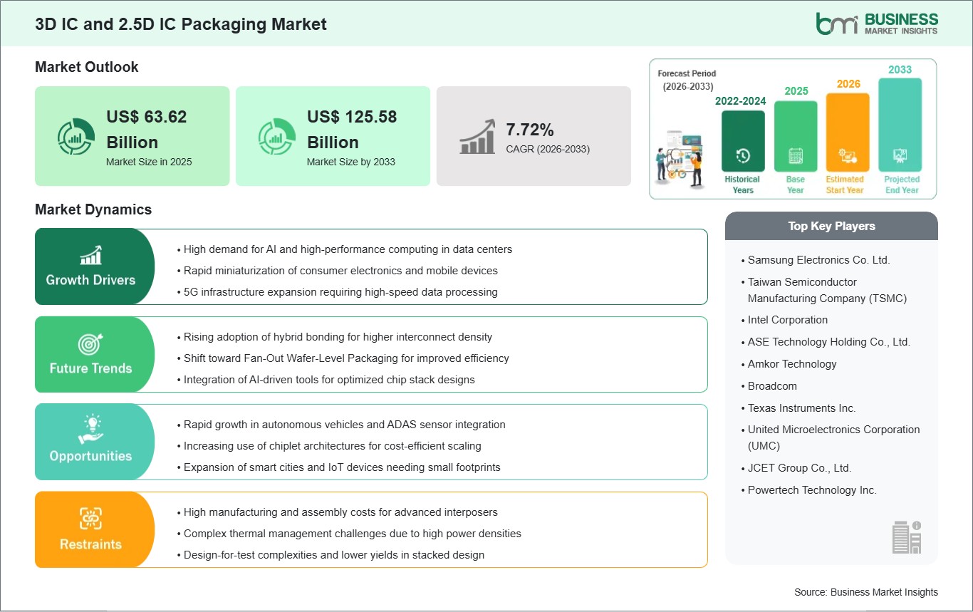
The 3D IC and 2.5D IC Packaging Market size is expected to reach US$ 125.58 Billion by 2033 from US$ 63.62 Billion in 2025. The market is estimated to record a CAGR of 8.87% from 2026 to 2033.
Executive Summary and Global Market Analysis:
3D and 2.5D IC Packaging represent the vanguard of semiconductor architecture, enabling the vertical and horizontal integration of multiple silicon dies into a single high-performance unit. These technologies are critical for overcoming the physical limitations of Moore's Law, offering significantly higher interconnect density, reduced latency, and improved power efficiency compared to traditional 2D layouts. By utilizing Through-Silicon Vias (TSVs) and silicon interposers, these packaging solutions facilitate the "More than Moore" era, essential for the next generation of high-performance computing (HPC), artificial intelligence (AI), and 5G infrastructure.
However, the industry faces substantial technical and economic restraints that could impact widespread adoption. The manufacturing process is inherently complex, requiring high-precision equipment for wafer thinning and hybrid bonding, which often leads to yield management challenges and high initial capital expenditure (CapEx). Thermal management remains a critical hurdle, as stacking active dies creates localized "hot spots" that require advanced cooling solutions to prevent performance degradation. Furthermore, supply chain sensitivities, such as long lead times for specialized manufacturing tools and geopolitical export controls on advanced packaging equipment, pose ongoing risks.
Despite these challenges, the market remains characterized by lucrative opportunities, particularly as the industry transitions to chiplet-based architectures and heterogeneous integration. The surge in demand for High-Bandwidth Memory (HBM) and the expansion of sovereign semiconductor ecosystems through government incentives, such as the CHIPS Act, ensure a robust growth trajectory for players capable of mastering these high-density integration techniques.
3D IC and 2.5D IC Packaging Market - Strategic Insights:
Get more information on this report
3D IC and 2.5D IC Packaging Market Segmentation Analysis:
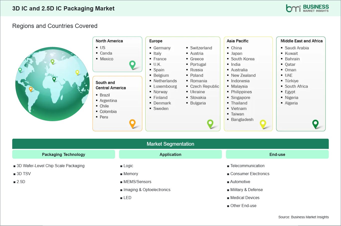
Key segments that contributed to the derivation of the 3D IC and 2.5D IC Packaging market analysis are packaging technology, application, and end-use.
By Packaging Technology, the market is segmented into 3D Wafer-Level Chip Scale Packaging (WLCSP), 3D TSV, and 2.5D.
By Application, the market is divided into Logic, Memory, MEMS/Sensors, Imaging &Optoelectronics, and LED.
By End-use, the market is categorized into Telecommunication, Consumer Electronics, Automotive, Military &Defense, Medical Devices, and Others.
3D IC and 2.5D IC Packaging Market Drivers and Opportunities:
Proliferation of Generative AI and High-Performance Computing (HPC)
The surging demand for Generative AI and High-Performance Computing (HPC) serves as the primary engine driving the 3D and 2.5D IC packaging market. Modern AI workloads, particularly those involving large language models (LLMs) like GPT-4, require massive data transfer speeds that traditional 2D architectures cannot sustain. Advanced packaging technologies, such as 2.5D interposers and 3D Through-Silicon Vias (TSVs), provide the critical vertical highway needed to couple high-performance GPUs with High-Bandwidth Memory (HBM) stacks.
By integrating memory and logic in a three-dimensional footprint, manufacturers can achieve bandwidths exceeding 1,000 GB/s, effectively breaking the "memory wall" that limits computational throughput. This vertical integration drastically shortens interconnect lengths, which not only reduces latency by several orders of magnitude but also lowers energy-per-bit consumption, a vital factor for hyperscale data centers facing rising operational costs. As compute intensity continues to double every few months, the industry is shifting its focus from transistor shrinkage (Moore's Law) toward advanced packaging as the primary lever for performance scaling. Consequently, major semiconductor firms and cloud service providers are making multi-billion-dollar capital commitments to secure advanced packaging capacity, ensuring sustained market momentum through 2033.
A transformative opportunity lies in the global transition toward chiplet-based architectures and heterogeneous integration. As the cost and complexity of manufacturing monolithic System-on-Chips (SoCs) on leading-edge nodes (3nm and beyond) become prohibitively high, the industry is moving toward a modular "LEGO-like" design philosophy. This involves disaggregating a large chip into smaller, functional "chiplets", such as logic, I/O, and memory, that can be manufactured on different, optimized process nodes and then reassembled into a single package.
This approach offers significant economic advantages, including drastically improved manufacturing yields and the ability to reuse proven IP blocks, which shortens time-to-market. The rise of standardized interconnect protocols, such as Universal Chiplet Interconnect Express (UCIe), allows for a multi-vendor ecosystem where designers can mix and match chiplets from different suppliers. This modularity is particularly lucrative for specialized sectors like Automotive ADAS, where sensor fusion and edge AI require high-density integration in compact, thermally efficient footprints. Furthermore, as the industry moves toward integrating hundreds, and eventually thousands, of chiplets into a single wafer-level system, the demand for precision bonding services and advanced redistribution layers (RDL) will create an expansive new revenue frontier for OSATs (Outsourced Semiconductor Assembly and Test) and foundries alike.
3D IC and 2.5D IC Packaging Market Size and Share Analysis:
The 3D IC and 2.5D IC Packaging market demonstrates steady growth, with size and share analysis revealing evolving trends and competitive positioning among key players. The report further examines subsegments categorized within packaging technology, application, and end-use, offering insights into their contribution to overall market performance.
For instance, the 3D TSV currently holds a dominant share in the technology segment due to its essential role in AI accelerators and HBM stacks.
Within the application category, Logic continues to lead the market, representing over half of the revenue as high-end processors transition to multi-die configurations to maintain performance scaling.
From an end-use perspective, Consumer Electronics remains the most significant volume contributor, fueled by the relentless demand for miniaturization in smartphones and wearables.
3D IC and 2.5D IC Packaging Market Report Highlights:
Australia, China, India, Japan, South Korea, Indonesia, Malaysia, Philippines, Singapore, Thailand, Vietnam, Bangladesh, New Zealand, Taiwan
South and Central America
Brazil, Argentina, Peru, Chile, Colombia
Middle East and Africa
Bahrain, Kuwait, Oman, Qatar, Saudi Arabia, United Arab Emirates, Turkiye, South Africa, Egypt, Algeria, Nigeria
Market leaders and key company profiles
Samsung Electronics Co. Ltd.
Taiwan Semiconductor Manufacturing Company (TSMC)
Intel Corporation
ASE Technology Holding Co., Ltd.
Amkor Technology
Broadcom
Texas Instruments Inc.
United Microelectronics Corporation (UMC)
JCET Group Co., Ltd.
Powertech Technology Inc.
Get more information on this report
3D IC and 2.5D IC Packaging Market Report Coverage and Deliverables:
The "3D IC and 2.5D IC Packaging Market Size and Forecast (2022 - 2033)" report provides a detailed analysis of the market covering below areas:
3D IC and 2.5D IC Packaging market size and forecast at global, regional, and country levels for all the key market segments covered under the scope
3D IC and 2.5D IC Packaging market trends, as well as market dynamics such as drivers, restraints, and key opportunities
3D IC and 2.5D IC Packaging market analysis covering key market trends, global and regional framework, major players, regulations, and recent market developments
Industry landscape and competition analysis covering market concentration, heat map analysis, prominent players, and recent developments for the 3D IC and 2.5D IC Packaging market
Detailed company profiles, including SWOT analysis
3D IC and 2.5D IC Packaging Market Geographic Insights:
The geographical scope of the 3D IC and 2.5D IC Packaging market report is divided into five regions: North America, Asia Pacific, Europe, the Middle East &Africa, and South &Central America.
In North America, the market is characterized by a strong emphasis on the research and design of high-end AI accelerators and the expansion of domestic advanced packaging facilities to secure critical semiconductor supply chains. The Asia-Pacific region serves as a core manufacturing hub, utilizing its extensive network of foundries and outsourced semiconductor assembly and test providers to support high-volume production. Europe maintains a specialized focus on the automotive and industrial sectors, where packaging solutions are developed to meet rigorous reliability and thermal management standards for vehicle safety systems. The Middle East &Africa are witnessing steady adoption through investments in digital infrastructure and data centers, while South &Central America are seeing a gradual increase in back-end assembly and testing activities for regional consumer markets. This regional diversity ensures that as global demand for miniaturized, high-performance electronics grows, each geography leverages its local expertise to contribute to the broader market expansion.
Get more information on this report
3D IC and 2.5D IC Packaging Market Research Report Guidance:
The report includes qualitative and quantitative data in the 3D IC and 2.5D IC Packaging market across packaging technology, application, end-use, and geography.
The report starts with the key takeaways (chapter 2), highlighting the key trends and outlook of the 3D IC and 2.5D IC Packaging market.
Chapter 3 includes the research methodology of the study.
Chapter 4 further includes ecosystem analysis.
Chapter 5 highlights the major industry dynamics in the 3D IC and 2.5D IC Packaging market, including factors that are driving the market, prevailing deterrents, potential opportunities, as well as future trends. Impact analysis of these drivers and restraints is also covered in this section.
Chapter 6 discusses the 3D IC and 2.5D IC Packaging market scenario, in terms of historical market revenues, and forecast till the year 2033.
Chapters 7 to 10 cover 3D IC and 2.5D IC Packaging market segments by packaging technology, application, end-use, and geography across North America, Europe, Asia Pacific, the Middle East and Africa, and South and Central America. They cover the market revenue, forecast, and factors driving the market.
Chapter 11 describes the competitive analysis along with the heat map analysis for the key players operating in the market.
Chapter 12 describes the industry landscape analysis. It provides detailed descriptions of business activities such as market initiatives, new developments, mergers, and joint ventures globally, along with a competitive landscape.
Chapter 13 provides detailed profiles of the major companies operating in the 3D IC and 2.5D IC Packaging market. Companies have been profiled on the basis of their key facts, business descriptions, products and services, financial overview, SWOT analysis, and key developments.
Chapter 14, i.e., the appendix, is inclusive of a brief overview of the company, a list of abbreviations, and a disclaimer.
3D IC and 2.5D IC Packaging Market News and Key Development:
The 3D IC and 2.5D IC Packaging market is evaluated by gathering qualitative and quantitative data post primary and secondary research, which includes important corporate publications, association data, and databases. A few of the key developments in the 3D IC and 2.5D IC Packaging market are:
In April 2025, Siemens Digital Industries Software announced that its continued collaboration with Intel Foundry resulted in multiple product certifications, updated foundry reference flows, and additional technology enablement. These achievements leveraged the foundry's leading-edge technologies for next-generation integrated circuits (IC) and 3D IC and 2.5D IC Packaging. As a founding partner of the Intel Foundry Accelerator Chiplet Alliance, Siemens enabled new and compelling solutions for 3D IC and chiplet offerings across a breadth of semiconductor market verticals.
In June 2025, TSMC announced the expansion of its 3DFabric advanced packaging platform, introducing enhanced CoWoS® and InFO® technologies to support high-performance computing and AI accelerators. The updated platform enables higher interconnect density, improved power efficiency, and greater design flexibility for chiplet-based architectures. This development strengthens TSMC’s capabilities in advanced 3D and 2.5D IC packaging to meet rising demand from data center, automotive, and next-generation semiconductor applications.
Key Sources Referred:
World Bank - Global Trade Indicators
World Trade Organization (WTO)
International Monetary Fund (IMF)
International Trade Administration (ITA)
Company website
Company annual reports
Company investor presentations
The List of Companies - 3D IC and 2.5D IC Packaging Market
Samsung Electronics Co. Ltd.
Taiwan Semiconductor Manufacturing Company (TSMC)
Intel Corporation
ASE Technology Holding Co., Ltd.
Amkor Technology
Broadcom
Texas Instruments Inc.
United Microelectronics Corporation (UMC)
JCET Group Co., Ltd.
Powertech Technology Inc.
Frequently Asked Questions
How big is the 3D IC and 2.5D IC Packaging Market?
The 3D IC and 2.5D IC Packaging Market is valued at US$ 63.62 Billion in 2025, it is projected to reach US$ 125.58 Billion by 2033.
What is the CAGR for 3D IC and 2.5D IC Packaging Market by (2026 - 2033)?
As per our report 3D IC and 2.5D IC Packaging Market, the market size is valued at US$ 63.62 Billion in 2025, projecting it to reach US$ 125.58 Billion by 2033. This translates to a CAGR of approximately 8.87% during the forecast period.
What segments are covered in this report?
The 3D IC and 2.5D IC Packaging Market report typically cover these key segments-
End-use (Telecommunication, Consumer Electronics, Automotive, Military & Defense, Medical Devices, Other End-use)
What is the historic period, base year, and forecast period taken for 3D IC and 2.5D IC Packaging Market?
The historic period, base year, and forecast period can vary slightly depending on the specific market research report. However, for the 3D IC and 2.5D IC Packaging Market report:
Historic Period : 2022-2024
Base Year : 2025
Forecast Period : 2026-2033
Who are the major players in 3D IC and 2.5D IC Packaging Market?
The 3D IC and 2.5D IC Packaging Market is populated by several key players, each contributing to its growth and innovation. Some of the major players include:
Samsung Electronics Co. Ltd.
Taiwan Semiconductor Manufacturing Company (TSMC)
Intel Corporation
ASE Technology Holding Co., Ltd.
Amkor Technology
Broadcom
Texas Instruments Inc.
United Microelectronics Corporation (UMC)
JCET Group Co., Ltd.
Powertech Technology Inc.
Who should buy this report?
The 3D IC and 2.5D IC Packaging Market report is valuable for diverse stakeholders, including:
Investors: Provides insights for investment decisions pertaining to market growth, companies, or industry insights. Helps assess market attractiveness and potential returns.
Industry Players: Offers competitive intelligence, market sizing, and trend analysis to inform strategic planning, product development, and sales strategies.
Suppliers and Manufacturers: Helps understand market demand for components, materials, and services related to concerned industry.
Researchers and Consultants: Provides data and analysis for academic research, consulting projects, and market studies.
Financial Institutions: Helps assess risks and opportunities associated with financing or investing in the concerned market.
Essentially, anyone involved in or considering involvement in the 3D IC and 2.5D IC Packaging Market value chain can benefit from the information contained in a comprehensive market report.


 Get Free Sample For 3D IC and 2.5D IC Packaging Market


